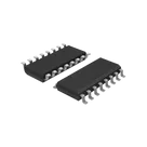
Pin Function Grouping

Started implementing a plan
#Goal
- Group the HX711 part pins from its datasheet by function, ensuring each pin is assigned exclusively to one of the following categories: regulator/power, ground, analog inputs, digital serial interface, clock, or control/reference.
#Implementation plan
1. **Review the HX711 datasheet pin table**
1. Refer to the provided datasheet (https://cdn.sparkfun.com/datasheets/Sensors/ForceFlex/hx711_english.pdf) and verify the pin table details for the 16-pin SOP package.
2. **Define functional groups based on pin functions**
1. Create the following groups:
- **Regulator/Power:** Pins supplying regulated voltages.
- **Ground:** The ground reference pin.
- **Analog Inputs:** Pins associated with analog measurements.
- **Digital Serial Interface:** Pins used for digital serial communication.
- **Clock:** Pins related to crystal clock input or clock generation.
- **Control/Reference:** Pins used for control signals and reference inputs/outputs.
3. **Assign each pin to a single group according to its datasheet function**
1. **Regulator/Power:**
- Pin 1: VSUP (regulator supply 2.7–5.5V)
- Pin 3: AVDD (analog supply 2.6–5.5V)
- Pin 16: DVDD (digital supply)
2. **Ground:**
- Pin 5: AGND (analog ground)
3. **Analog Inputs:**
- Pin 7: INA- (Channel A negative input)
- Pin 8: INA+ (Channel A positive input)
- Pin 9: INB- (Channel B negative input)
- Pin 10: INB+ (Channel B positive input)
4. **Digital Serial Interface:**
- Pin 12: DOUT (serial data output)
5. **Clock:**
- Pin 13: XO (crystal I/O)
- Pin 14: XI (crystal I/O or external clock input)
6. **Control/Reference:**
- Pin 2: BASE (regulator control output)
- Pin 4: VFB (regulator control input)
- Pin 6: VBG (reference bypass output)
- Pin 11: PD_SCK (power-down control and serial clock input)
- Pin 15: RATE (data rate control input)
4. **Audit the grouping for compliance**
1. Verify that all 16 pins are present.
2. Ensure no pin appears in more than one group and every pin is exclusively assigned to its designated function group.
#Success criteria
- All 16 HX711 pins are assigned to one and only one of the groups: regulator/power, ground, analog inputs, digital serial interface, clock, or control/reference.
- The assignment strictly follows the datasheet pin definitions without duplications or omissions.
Task completed.
0:43
HX711