Part Data Review and Update
Thought for 3 mins 30 sec
I reviewed the current part data and compared it against the datasheet-driven audit workflow, where the datasheet is the source of truth for pin identity/count and project properties should be updated using the exact existing property names to avoid duplicates
Summary
Table
| Item | Current project | Datasheet / audit finding | Status |
|---|---|---|---|
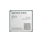
| MPN | EC21EFA-512-STD | Variant of Quectel EC21 series | Mostly OK |
| Manufacturer | Quectel | Quectel Wireless Solutions Co., Ltd. | OK |
| Datasheet URL | Present already | URL exists, so no web search/update was required | OK |
| Package | Module | LCC package, 32.0 mm x 29.0 mm x 2.4 mm | Too generic |
| Description | LTE Category 1 Module 3.8V LCC | Reasonable, but could be more specific | Acceptable |
| Supply | Not in properties shown | 3.3 V to 4.3 V, 3.8 V typ | Missing from part metadata |
| Temperature | Not in properties shown | -35 C to +75 C, extended -40 C to +85 C | Missing from part metadata |
| LTE category | In description only | LTE Cat 1 | OK |
| Physical pad count | Layout/symbol model shows 132 pads/terminals | Datasheet package has 144 pads total | Needs interpretation |
| Pin typing | Sampled terminals all show Pin Type: Unspecified | Datasheet provides enough info to map types | Mismatch |
| Pin descriptions | Not visible on sampled terminals | Datasheet provides functions/descriptions | Missing/incomplete |
- Cellular module: LTE Cat 1
- Data rate: up to 10 Mbps downlink / 5 Mbps uplink
- Supply: 3.3 V to 4.3 V, 3.8 V typical
- Temperature: -35 C to +75 C, extended -40 C to +85 C
- Package: LCC, 32.0 mm x 29.0 mm x 2.4 mm
- Package pad structure: 144 total pads made up of 80 LCC + 64 LGA/other pads
- The part already has a Datasheet URL set, so your “if missing, find one and update it” condition does not apply here.
- I did not need to search the web.
- The schematic currently contains 132 terminal components.
- The datasheet package has 144 total pads.
- However, the datasheet also marks pins 73-84 as reserved keepout pads that “should not be designed in schematic/PCB.” That is 12 pads, and 144 - 12 = 132.
- So the current 132-terminal model appears internally consistent if your intent is to omit the keepout-only reserved pads. The sync guidance normally says to match datasheet pin count exactly unless there is a documented reason not to, and this looks like one of those documented exceptions
I found clear evidence that the symbol is not fully aligned to the datasheet pin names:
- AP_READY and PCM_IN are present with expected names.
- But multiple datasheet-defined pins were not found by their official names in the project search, including signals like
USB_BOOT, theSDC2_*group,VDD_SDIO,SD_INS_DET, Bluetooth/WLAN coexistence pins, and several Ethernet/SGMII pins. - That strongly suggests those pads are currently represented as generic
RESERVED_*terminals or otherwise renamed.
- The sampled terminals I inspected, such as ADC1, PWRKEY, and USB_VBUS, all show
Pin Type: Unspecified. - For an IC/module part like this, that is a significant metadata gap. The recommended sync workflow is to assign exact
Pin Number,Pin Type, shortPin Description, plusSection,Pin Group, andPin Orientationwhere applicable - I also did not see pin-description properties in the sampled terminal data, so those appear to be missing or incomplete.
- The layout contains a footprint with 132 pads, matching the current symbol representation.
- From the available layout output, I can confirm the footprint exists and pad identities are present, but I cannot fully verify pad geometry, pad sizes, or XY placement against the recommended land pattern because the tool output here did not include the detailed footprint dimensions.
- So:
- Pad-count consistency: looks OK for the 132-pad usable-pin interpretation
- Mechanical land-pattern accuracy: not fully verified yet
- Symbol terminal names are partially wrong or too generic
- Pin types are unassigned
- Pin descriptions are missing/incomplete
- Package property is too generic (
Moduleinstead of a clearer LCC package designation) - Electrical metadata like operating voltage and temperature range are not populated
- Footprint geometry was not fully verifiable from the data returned
I can perform the cleanup pass next:
- normalize the project properties,
- preserve the existing Datasheet URL,
- and align the terminal metadata to the datasheet naming/type conventions without creating duplicate properties
To get started, talk to Flux or create a New Document.


Welcome 👋
Flux accelerates your PCB design with AI.
Create your account to start using this component and bring your ideas to life.