Part Review and Datasheet Verification
Thought for 4 sec
I’ll update each terminal with datasheet-based pin metadata: number, name/designator, type, functional group/section, and description, then verify the schematic properties.
Worked for 1 min 25 sec
Metadata was applied; I’m normalizing a few fields to Flux standard property names/options where possible while keeping the datasheet grouping intent.
Worked for 1 min 9 sec
Added datasheet-based metadata to all 22 E04-400M16S terminals and verified the updates. Each pin now has Pin Number, Pin Role/name, Pin Type, Pin Group, Section, and Pin Description; I used one primary group per pin and normalized pin types to Flux standard values where available.
Open items:
- The symbol is still represented as 22 separate Terminal components rather than one module component.
- SPI MISO/MOSI directions follow the EBYTE datasheet wording, which should be rechecked against host/module convention during integration.
Suggested next steps:
- Convert these terminals into a single 22-pin module symbol.
- Correct and verify the footprint pad coordinates against the official EBYTE package.
- Add VCC decoupling and RF/antenna layout constraints.
Fix symbol and footprint
Create module symbol
Fix footprint pads
Add support circuitry
Run design review
Refine this doc
Ask about this doc
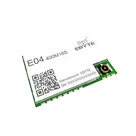
Part Information Review — E04-400M16S
Date: 2026-06-23
Scope
Reviewed available project part information for EBYTE / Chengdu Ebyte E04-400M16S, including MPN, manufacturer, package/mechanical data, pin count, description, project properties, schematic terminals, symbol pin descriptions, and PCB footprint geometry. Cross-check source was the project Datasheet URL plus official EBYTE/CDEBYTE web product pages found during review.
Current Project Part Information
Project-level properties
- Manufacturer Part Number: E04-400M16S
- Manufacturer Name: EBYTE
- Part Type: Module
- Designator Prefix: U
- Datasheet URL: c20809641fc95c369cb0c0cf314b91395e6db3930a532fce3a7d243b1af747fd.pdf
- Symbol Style: parametric-v1
- License: https://creativecommons.org/licenses/by/4.0/
Schematic representation
- Current schematic is represented as 22 separate
Terminalcomponents rather than one integrated module symbol. - All 22 terminal entries use the same Terminal part UID.
- No nets are currently defined.
- Pin numbers present: 1 through 22.
- Pin names/designators present: GND pins, GPIO0, GPIO1, GPIO2, GPIO3, VCC, SDN, NC, MISO, MOSI, SCLK, CSN, ANT.
PCB footprint representation
- Footprint uses 22 top-layer rectangular SMD pads.
- Global pad rule: rectangular pad, 1.7 mm × 1.0 mm.
- Body/silk outline: rectangle from approximately -7,-10 mm to +7,+10 mm, matching a 14 mm × 20 mm module outline.
- Pad placement is incomplete/irregular: most pads are positioned, but SDN has no explicit position rule and computes to 0,0.
Datasheet / Official Source Key Specs
- Part: E04-400M16S
- Manufacturer: Chengdu Ebyte Electronic Technology Co., Ltd / EBYTE
- Core RF IC: ST S2-LP / S2-LPQTR
- Function: 433/470 MHz low-power SMD RF transceiver module, SPI-controlled
- Frequency range: 413–479 MHz
- Typical frequency: 433 MHz
- Operating voltage: 2.5–3.6 V, typ. 3.3 V; ≥3.3 V recommended for guaranteed output power
- Logic level: 3.3 V; 5 V TTL risks damage unless protected
- TX current: typ. 10 mA at 10 dBm
- RX current: typ. 7 mA
- Sleep current: typ. 2.5 nA
- Max TX power: up to 16 dBm
- Receiver sensitivity: down to -130 dBm at 0.3 kbps; commonly -100 to -120 dBm depending conditions
- Air data rate: 0.3–250 kbps depending modulation
- Modulations: 2(G)FSK, 4(G)FSK, OOK, ASK / SIGFOX support noted
- SPI interface: 0–10 Mbps
- Operating temperature: -40 to +85 °C
- Module size: 20 mm × 14 mm
- Package/interface: SMD castellated/stamp-hole, 1.27 mm pitch
- RF interface: stamp-hole ANT and/or IPEX, about 50 Ω
- Recommended hardware notes: add ceramic filter capacitor at VCC; keep high-frequency/power routing away from/under module; use stable low-ripple supply; keep antenna exposed and avoid metal enclosure shielding.
Datasheet Pinout Cross-Check
Table
| Pin | Datasheet name | Datasheet direction | Datasheet function | Project terminal present | Match |
|---|---|---|---|---|---|
| 1 | GND | — | Ground | GND | OK |
| 2 | GND | — | Ground | GND | OK |
| 3 | GND | — | Ground | GND | OK |
| 4 | GND | — | Ground | GND | OK |
| 5 | GND | — | Ground | GND | OK |
| 6 | GPIO1 | I/O | Configurable GPIO | GPIO1 | OK |
| 7 | GPIO2 | I/O | Configurable GPIO | GPIO2 | OK |
| 8 | GPIO3 | I/O | Configurable GPIO | GPIO3 | OK |
| 9 | VCC | — | 2.5–3.6 V supply | VCC | OK |
| 10 | GND | — | Ground | GND | OK |
| 11 | GND | — | Ground | GND | OK |
| 12 | GND | — | Ground | GND | OK |
| 13 | GPIO0 | I/O | Configurable GPIO | GPIO0 | OK |
| 14 | SDN | Input | Shutdown control | SDN | OK name, but footprint pad position missing |
| 15 | NC | — | No connect | NC | OK |
| 16 | MISO | Input | SPI data input pin per datasheet wording | MISO | OK name; verify host/module direction convention before schematic use |
| 17 | MOSI | Output | SPI data output pin per datasheet wording | MOSI | OK name; verify host/module direction convention before schematic use |
| 18 | SCLK | Input | SPI clock input | SCLK | OK |
| 19 | CSN | Input | SPI chip select | CSN | OK |
| 20 | GND | — | Ground | GND | OK |
| 21 | ANT | — | 50 Ω antenna interface | ANT | OK |
| 22 | GND | — | Ground | GND | OK |
Mismatches / Issues Flagged
- Symbol architecture mismatch: The part is modeled as 22 independent Terminal components rather than a single module component. This makes BOM, symbol review, pin properties, pin grouping, and footprint association fragile.
- Pin descriptions/types mostly missing: Most terminals only have
Pin Type: Unspecifiedor no descriptive pin metadata. Datasheet direction/function information is not encoded in the symbol properties. - Footprint pad placement error: SDN pad has no explicit position rule and resolves to 0,0, which is inconsistent with the datasheet pinout and the other pads.
- Footprint geometry needs verification: Module outline matches 14 × 20 mm and pad size appears plausible, but current pad coordinates do not form a clear 1.27 mm castellated perimeter pattern from the datasheet. Several signal pads appear irregularly placed relative to expected module edges.
- Pad numbering/identity is indirect: Pads are named by terminal designator and UID rather than a clean numbered pad map tied to one module footprint, making mechanical/pin verification error-prone.
- No schematic nets: There are no nets, so electrical connectivity cannot be validated beyond symbol/terminal presence.
- Datasheet URL already existed: Per user instruction, no datasheet property update was required. Official web sources found include EBYTE product page
https://www.ebyte.com/product/1047.htmland CDEBYTE English product pagehttps://www.cdebyte.com/products/E04-400M16S/2.
Recommended Fixes
- Convert the 22 terminals into a single E04-400M16S module component with 22 pins.
- Add pin metadata from the datasheet: pin number, pin name, pin direction/type, section/group, and pin description.
- Rebuild or correct the footprint against the official EBYTE package/footprint download and datasheet mechanical drawing.
- Explicitly position SDN pad and verify all pad coordinates against the 20 × 14 mm, 1.27 mm castellated footprint.
- Add VCC decoupling guidance/property notes: ceramic filter capacitor close to VCC/GND.
- Treat ANT as a 50 Ω RF node and keep copper/routing around the module/antenna region consistent with EBYTE antenna guidance.
Scope
Current Project Part Information
Project-level properties
Schematic representation
PCB footprint representation
Datasheet / Official Source Key Specs
Datasheet Pinout Cross-Check
Mismatches / Issues Flagged
Recommended Fixes