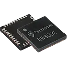
Parts Datasheet Verification
Thought for 3 mins 59 sec
Part review completed
2) Datasheet source used for scan
Key features
4) Absolute maximum ratings
5) Recommended / nominal operating conditions
6) Selected electrical characteristics
7) Pin-function summary
Power, RF, clock, and control pins
SPI and GPIO
8) Package / mechanical information
9) Layout guidance from datasheet
10) Symbol and footprint cross-check
Good matches
Issues and flags
11) Bottom line
12) Recommended fixes
The datasheet property was already set, so no web-found replacement URL needed to be written back.
1) Current part metadata review
Table
| Field | Current value | Status |
|---|---|---|
| MPN | DW3210TR13 | Present |
| Manufacturer | Qorvo | Present |
| Description | IC RF TxRx Only 802.15.4 IR-UWB 6.5 GHz, 8 GHz 40-WFQFN Exposed Pad | Present |
| Part type | Integrated Circuits | Present |
| Datasheet URL | https://www.qorvo.com/products/d/da008142 | Present |
| Symbol pin count | 40 terminals | Present |
| Footprint pad count | 40 pads | Present |
| Package metadata field | Not explicitly set as a structured package property in the part metadata I could read | Incomplete |
| Pin electrical types | All terminals currently show Unspecified | Incomplete |
The existing Qorvo URL was set, but it did not return clean structured results consistently through file scanning. I therefore used a directly accessible datasheet PDF mirror of the same DW3000-family datasheet to complete the extraction:
- Datasheet used for detailed extraction:
https://www.mouser.com/catalog/specsheets/Qorvo_DW3000.pdf
Table
| Item | Datasheet result |
|---|---|
| Family | DW3000 UWB Transceiver |
| Variant | DW3210 |
| Package | QFN40 |
| Package size | 5 mm x 5 mm |
| Pin count | 40 pads |
| Temperature grade | -40 °C to +85 °C |
| Channels | 5 and 9 |
| Center frequencies | 6489.6 MHz and 7987.2 MHz |
| SPI | Up to 38 MHz |
| Data rates | 850 kbps and 6.8 Mbps |
Table
| Feature | Datasheet result |
|---|---|
| UWB standard | IEEE 802.15.4-2015 and IEEE 802.15.4z (BPRF mode) |
| Location modes | 2-way ranging, TDoA, PDoA |
| Security | Integrated HW AES 256 |
| Power | Low power consumption |
| Packet length | Up to 1023 bytes |
| Package options in family | QFN40 (5 mm x 5 mm) and WLCSP52 (3.1 mm x 3.5 mm) |
Table
| Parameter | Min | Max | Units |
|---|---|---|---|
| Supply voltage | -0.3 | 4.0 | V |
| Receiver power | 14 | dBm | |
| Storage temperature | -65 | +150 | °C |
| Operating temperature | -40 | +85 | °C |
| MSL for QFN packages | 3 | 3 | Level |
| ESD, HBM | 2000 | V |
Table
| Parameter | Min | Typ | Max | Units |
|---|---|---|---|---|
| Operating temperature | -40 | 85 | °C | |
| Supply voltage VDD1 | 1.62 | 3.0 | 3.6 | V |
| Supply voltage VDD2a / VDD2b | 2.4 | 3.0 | 3.6 | V |
| Supply voltage VDD3 | 1.5 | 3.0 | 3.6 | V |
| Voltage on GPIO0-5, WAKEUP, RSTn, SPICSn, SPIMOSI, SPICLK | 3.6 | V |
Table
| Parameter | Value |
|---|---|
| Deep sleep current | 260 nA |
| Sleep current | 850 nA |
| Idle current, channel 5 | 18 mA |
| Idle current, channel 9 | 32 mA |
| Idle-RC current | 8 mA |
| Oscillator startup current | 1.5 mA |
| Single TX frame current, CH5 | 14 mA |
| Single TX frame current, CH9 | 17 mA |
| Single RX frame current, CH5 | 16 mA |
| Single RX frame current, CH9 | 19 mA |
| Peak RX current, CH5 | 72 mA |
| Peak RX current, CH9 | 88 mA |
| Peak TX current, CH5 VDD2 | 23 mA nominal, 29 mA max power |
| Peak TX current, CH9 VDD2 | 24 mA nominal, 29 mA max power |
| Peak TX current, CH5 VDD3 | 25 mA |
| Peak TX current, CH9 VDD3 | 35 mA |
| Receiver sensitivity example, CH5, 850 kbps | -100 dBm / 500 MHz |
| Receiver sensitivity example, CH5, 6.8 Mbps | -94.3 dBm / 500 MHz |
| Output power spectral density | -31 dBm/MHz |
| RF load impedance | 50 Ω single-ended |
Table
| Pin group | Datasheet summary |
|---|---|
| RF1 | 50 Ω single-ended RF connection, requires 2 pF on the pin |
| RF2 | 50 Ω single-ended RF connection; for non-PDoA variants it should be grounded with 50 Ω, and a 50 Ω PCB trace is required |
| XTI / XTO | Reference crystal input / output |
| VDD1 | Main supply, 1.62 V to 3.6 V, also powers several digital I/Os |
| VDD2a / VDD2b | Supply, 2.4 V to 3.6 V |
| VDD3 | Supply, 1.5 V to 3.6 V |
| VTX_D | TX supply decoupling, requires external capacitor to ground |
| VIO_D | I/O supply decoupling |
| WAKEUP | Active-high wake input; connect to ground if unused |
| RSTn | Active-low reset; must not be pulled high by external source |
| EXTON | External enable output for external power circuitry |
| IRQ | Interrupt output; recommended external 100 kΩ pull-down to avoid spurious interrupts in sleep/deepsleep |
Table
| Pin group | Datasheet summary |
|---|---|
| SPICLK / SPICSn / SPICDI / SPICDO | SPI interface |
| GPIO0-8 | GPIOs with alternate LED / control / sync functions |
| GPIO5 / GPIO6 at power-up | Define SPI polarity and SPI phase configuration on startup |
| LED note | GPIO pins are not suitable to drive LEDs directly |
Table
| Item | Datasheet result |
|---|---|
| QFN package size | 5 mm x 5 mm |
| QFN package type | QFN40 |
| Reel size | 330 mm (13 in) |
| Units per reel, QFN | 4000 |
| QFN MSL | 3 |
Table
| Topic | Datasheet guidance |
|---|---|
| Trace length | Keep all traces as short as possible |
| Grouping | Avoid mixing RF, power, and digital groups together |
| Decoupling | Place decoupling capacitors as close as possible to the corresponding pads |
| RF lines | RF1 and RF2 should be 50 Ω impedance-controlled |
| DC-blocking capacitors | The 2 pF capacitor pads should be embedded into the RF track width |
| Copper clearance | Keep clear of copper, tracks, and vias around the RF structures shown in the recommended layout |
Table
| Check | Result | Risk |
|---|---|---|
| Symbol pin count vs datasheet | 40 vs 40 | Low |
| Footprint pad count vs datasheet | 40 vs 40 | Low |
| Pin numbering continuity | Appears consistent from 1 to 40 | Low |
| Major pin naming | Appears aligned with datasheet naming | Low |
Table
| Finding | Why it matters | Severity |
|---|---|---|
Footprint asset name is DW3220TR13-1.kicad_mod while the part MPN is DW3210TR13 | Even if the package is likely shared within the family, this creates a real risk of part-library confusion, wrong future substitutions, or incorrect trust in the footprint provenance | Medium |
Project description says 40-WFQFN Exposed Pad, but the footprint I inspected has only 40 perimeter pads and no obvious exposed center pad | If the actual DW3210 package truly requires an exposed pad, this would be a manufacturing and thermal/reliability issue. The datasheet excerpts I could access identify the device as QFN40 5 mm x 5 mm, but I did not get a machine-readable package drawing confirming a center pad one way or the other | High - needs manual verification against the package drawing |
All symbol terminals are typed Unspecified | Not a fabrication failure by itself, but it weakens ERC usefulness and can hide integration mistakes in downstream designs | Low |
| No structured package property visible in part metadata | Increases ambiguity during reuse and review | Low |
| Existing datasheet URL is not ideal for direct automated extraction | Makes future automated review less reliable | Low |
Table
| Area | Verdict |
|---|---|
| Basic symbol-to-datasheet pin mapping | Looks broadly correct |
| Basic footprint pad count / package family alignment | Looks broadly correct |
| Most important risk | Potential mismatch around exposed-pad status |
| Second important risk | Footprint file name references DW3220, not DW3210 |
Table
| Priority | Action |
|---|---|
| 1 | Verify the package drawing page for the DW3210 QFN40 and confirm whether there is an exposed center pad |
| 2 | If no exposed pad exists, update the part description to remove Exposed Pad |
| 3 | Rename or replace the footprint asset so its identity matches DW3210TR13 cleanly |
| 4 | Add proper pin electrical types for better rule checking |
| 5 | Replace the current datasheet property with a direct PDF URL if you want future automated scans to be more reliable |
If you want, I can next turn this into a concise pass/fail checklist for publishing the part.
Create publish checklist
Check exposed pad
Fix datasheet URL
Review pin types
To get started, talk to Flux or create a New Document.