Part Datasheet Review and Updates

Review all available part information (MPN, package, pin count, description, properties). If no datasheet URL is already set, search the web for the official datasheet and update the part's Datasheet property with the URL. Then cross-check the schematic symbol, footprint, and pin descriptions against the datasheet. Summarize key specs and flag any mismatches.
2:23
Thought for 3s
Read BOM.
Read schematic.
Read layout.
Read layout.
Search DS90UB953-Q1 datasheet RHB 32 VQFN pin description DS90UB953TRHBRQ1 PDF Texas Instruments.
Thought for a moment
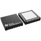
I reviewed the part against TI’s official DS90UB953-Q1 information; the Datasheet URL was already set, so I did not change it. The pin names/count mostly match, but I flagged property/metadata issues including EPAD typed as unspecified, RES1 typed as input, I²C pins typed as output, LPF pins unspecified, and missing richer part properties/descriptions. Full review is in DS90UB953TRHBRQ1 Part Datasheet Review.
Looking at the datasheet of this component, can you group together pins by their functions? for example for Power, VDD etc
NOTE: If you group them, can you not add the same pin if you already added them in a group? You should know which pin function is common for its function
2:30
Thought for 8s
Read schematic.
I grouped every DS90UB953-Q1 terminal into exactly one functional group: Power, Ground/Thermal, MIPI CSI-2 Input, FPD-Link III, I²C, GPIO, Clock, Control, Loop Filter, and Reserved. I also flagged current property fixes like
EPAD → Ground and I2C_SDA/SCL → Bi-Directional; full details are in DS90UB953-Q1 Pin Functional Groups.Fix pin metadata
Show wrong types
Symbol grouping plan
Check reserved pins
Ready to work


Welcome 👋
Flux accelerates your PCB design with AI.
Create your account to start using this component and bring your ideas to life.