Part Datasheet Review and Validation
0:52
Considering designator use.
Analyzing the schematic.
Reviewing the bill of materials.
Analyzing the PCB layout.
Looking for "part description, ordering information, package style, number of positions, terminal names" in 1810151213_Diptronics-DM-02-V-T-R_C225004.pdf
Looking for "absolute maximum ratings" in 1810151213_Diptronics-DM-02-V-T-R_C225004.pdf
Looking for "electrical characteristics" in 1810151213_Diptronics-DM-02-V-T-R_C225004.pdf
Looking for "recommended operating conditions" in 1810151213_Diptronics-DM-02-V-T-R_C225004.pdf
Looking for "pin configuration and terminal description" in 1810151213_Diptronics-DM-02-V-T-R_C225004.pdf
Looking for "mechanical dimensions and package dimensions" in 1810151213_Diptronics-DM-02-V-T-R_C225004.pdf
Looking for "special features, materials, contact rating, insulation resistance, dielectric strength, contact resistance, operating force, travel" in 1810151213_Diptronics-DM-02-V-T-R_C225004.pdf
Identifying temperature discrepancies.
https://datasheet.lcsc.com/lcsc/1810151213_Diptronics-DM-02-V-T-R_C225004.pdf
Part metadata found
Datasheet summary
| Category | Extracted details |
|---|---|
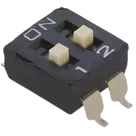
| Device type | 2-position SPST slide DIP switch |
| Mounting/package | SMD-4P, about 6.2 mm x 6.0 mm body |
| Pitch | 2.54 mm |
| Contact rating | 25 mA, 24 VDC |
| Contact resistance | 50 mOhm max initial |
| Insulation resistance | 100 MOhm min at 500 VDC |
| Dielectric strength | Reported as 300 VAC for 1 minute in one extract, and 500 VAC for 1 minute in another extract |
| Electrical life | 2,000 operations per switch |
| Storage temperature | -40 C to +85 C |
| Operating temperature | Reported as -20 C to +85 C in one extract, and -20 C to +70 C in another extract |
| Operating force | Reported as 500 gf max in one extract, and 1,000 gf max in another extract |
| Travel | 1 mm |
| Special features | Low profile, gold contact, top tape type for washing process |
Pin / terminal interpretation
| Schematic terminal | Pin number | Current meaning in project | Datasheet confidence |
|---|---|---|---|
| COM_1 | 1 | Common for switch 1 | Reasonable, but not explicitly confirmed from extracted pin table |
| COM_2 | 2 | Common for switch 2 | Reasonable, but not explicitly confirmed from extracted pin table |
| NO_1 | 3 | Switched contact for switch 1 | Reasonable, but not explicitly confirmed from extracted pin table |
| NO_2 | 4 | Switched contact for switch 2 | Reasonable, but not explicitly confirmed from extracted pin table |
- 4 SMD pads
- Pad centers at about
x = +/-1.27 mm,y = +/-4.45 mm - Pad size about 1.10 mm x 1.50 mm
- Body outline about 6.02 mm x 6.2 mm
Mismatches and risk flags
| Severity | Finding | Why it matters |
|---|---|---|
| High | Project package/case code is DIP, but datasheet/footprint indicate SMD-4P | This can cause incorrect part ordering, wrong filtering in library/BOM workflows, and confusion during manufacturing handoff |
| Medium | Terminal naming in the schematic is inferred as COM / NO, but the extracted datasheet text did not return a definitive per-pin table | If pin numbering is reversed relative to the manufacturer drawing, the symbol could map incorrectly to the footprint |
| Medium | Datasheet extracts contain conflicting values for dielectric strength, operating temperature, and operating force | These should be checked directly on the source PDF page before final publishing or release |
| Low | Terminal pin types are all currently Unspecified in the schematic | Not usually fatal for a switch part, but clearer terminal typing improves reuse and review quality |
- The footprint looks plausibly correct for a 4-pin SMD 2-position switch.
- The biggest issue is the package metadata mismatch: the part is marked DIP in project properties, while the datasheet and footprint indicate SMD-4P.
- The next biggest risk is pin mapping certainty. The current 4-terminal symbol is structurally reasonable, but I do not have a definitive extracted manufacturer pin table from the PDF text to prove the numbering/order is exact.


Welcome 👋
Flux accelerates your PCB design with AI.
Create your account to start using this component and bring your ideas to life.
