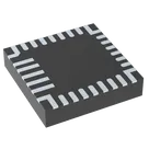
Part Data Review and Audit

Looking at the datasheet of this component, can you group together pins by their functions? for example for Power, VBUS, GND etc
Also can you place them into their respective sections based on their functions
NOTE: If you group them, can you not add the same pin if you already added them in a group? You should know which pin function is common for its function
Thought for 14 sec
I’ll group each existing terminal exactly once by its primary datasheet function, then set both the functional group and section properties on the symbol terminals and verify the result.
Worked for 2 mins 1 sec
Done — I assigned every existing terminal to exactly one datasheet-based functional group and a broad section, then verified the updates.
Examples: VBUS pins are grouped as Power Input, GND as Ground, SCL/SDA as I2C Interface, D+/D− as USB Data Detection, BAT/BATP as battery-related groups, and SW/BTST pins under switching/driver groups. Duplicate package lands like STAT_2, VAC1_2, TS_2, and SDRV_2 were kept in their matching primary function group and described as duplicate lands, not separate logical pins.
Run ERC/DRC
Show pin groups
Fix ambiguities
Check unused pins
Refine this doc
Ask about this doc
BQ25792RQMR Part Audit
Date: 2026-05-20
Sources Reviewed
- Project: BQ25792RQMR
- Official TI datasheet: https://www.ti.com/lit/ds/symlink/bq25792.pdf
- Datasheet title: BQ25792 I2C Controlled, 1-4 Cell, 5-A Buck-Boost Battery Charger with Dual-Input Selector and USB PD 3.0 OTG Output
- Datasheet revision: SLUSDG1C, Rev. C, June 2020 - Revised August 2022
- Package addendum date observed: 13-Apr-2026
Project Metadata Reviewed
- Project name: BQ25792RQMR
- Description after update: Charger IC Lithium Ion/Polymer 29-VQFN-HR (4x4)
- Datasheet URL property: added as https://www.ti.com/lit/ds/symlink/bq25792.pdf
- Implementation Details property: updated with official datasheet URL and package summary
- Assets present:
BQ25792RQMR Symbol.svg- default symbol/thumbnailBQ25792RQMR.kicad_mod- footprint assetBQ25792RQMR.stp- 3D model asset
Key Datasheet Specs
Table
| Parameter | Datasheet value |
|---|---|
| Function | I2C controlled buck-boost charger for 1-4 cell Li-ion / Li-polymer batteries |
| Charge current | 5 A, 10 mA resolution |
| Input operating voltage | 3.6 V to 24 V |
| Input absolute maximum | 30 V on VAC1, VAC2, VBUS when converter not switching |
| Battery charge voltage regulation range | 3 V to 18.8 V typical |
| OTG output voltage range | 2.8 V to 22 V, 10 mV resolution |
| OTG output current regulation | Up to 3.32 A, 40 mA resolution |
| Switching frequencies | 750 kHz or 1.5 MHz |
| I2C address | 7-bit address 0x6B |
| I2C bus speed | Standard mode up to 100 kbit/s and fast mode up to 400 kbit/s in serial interface text; electrical table also lists fSCL 1000 kHz |
| Package | VQFN-HR (RQM), 29 logical pins, 4 mm x 4 mm, 1 mm max height |
| Operating temperature | -40 C to 85 C ambient; -40 C to 125 C junction recommended operating condition |
| MSL / reflow | Level-2-260C-1 YEAR |
| Marking | BQ25792 |
Datasheet Pin Table vs Current Symbol Terminals
The datasheet defines 29 logical pins. The package mechanical/land pattern shows 33X terminals/lands. The current Flux symbol exposes 33 terminal components, matching the land count rather than the 29 logical datasheet pin count.
Table
| Datasheet pin | Datasheet name | Current symbol terminal(s) | Status |
|---|---|---|---|
| 1 | STAT | STAT_1 plus extra STAT_2 at symbol pin number 30 | Mismatch: extra terminal uses non-datasheet pin number 30 |
| 2-3 | VBUS | VBUS_1, VBUS_2 | OK; split logical pin range represented as two pads |
| 4 | BTST1 | BTST1 | OK |
| 5 | REGN | REGN | OK |
| 6 | D+ | D+ | OK |
| 7 | D- | D- | OK |
| 8 | VAC2 | VAC2 | OK |
| 9 | VAC1 | VAC1_1 plus extra VAC1_2 at symbol pin number 31 | Mismatch: extra terminal uses non-datasheet pin number 31 |
| 10 | ACDRV2 | ACDRV2 | OK |
| 11 | ACDRV1 | ACDRV1 | OK |
| 12 | QON | ~QON | Acceptable naming style; active-low marker may be misleading because datasheet calls it QON and describes low-duration functions, not a continuously active-low output |
| 13 | CE | ~CE | Acceptable active-low marker; datasheet states active-low charge enable |
| 14 | SCL | SCL | OK |
| 15 | SDA | SDA | OK |
| 16 | TS | TS_1 plus extra TS_2 at symbol pin number 32 | Mismatch: extra terminal uses non-datasheet pin number 32 |
| 17 | ILIM_HIZ | ILIM_HIZ | OK |
| 18 | BATP | BATP | OK |
| 19 | BTST2 | BTST2 | OK |
| 20 | PROG | PROG | OK |
| 21 | INT | ~INT | Acceptable active-low/open-drain marker; datasheet says active-low 256 us interrupt pulse |
| 22-23 | BAT | BAT_1, BAT_2 | OK; split logical pin range represented as two pads |
| 24 | SDRV | SDRV_1 plus extra SDRV_2 at symbol pin number 33 | Mismatch: extra terminal uses non-datasheet pin number 33 |
| 25 | SYS | SYS | OK |
| 26 | SW2 | SW2 | OK |
| 27 | GND | GND | OK |
| 28 | SW1 | SW1 | OK |
| 29 | PMID | PMID | OK |
Footprint / Package Cross-Check
- Datasheet package: RQM0029A, VQFN-HR, 29 logical pins, 4 mm x 4 mm, 1 mm max height.
- Datasheet package/land-pattern callout includes 33X mechanical terminals/lands.
- Project footprint asset exists: BQ25792RQMR.kicad_mod.
- Project layout exposes 33 pad nodes, matching the datasheet mechanical/land-pattern 33X count.
- The part project description currently matches the package family and size: 29-VQFN-HR (4x4).
Conclusion: the footprint pad count appears plausible for the TI RQM VQFN-HR package because the datasheet mechanical drawing uses 33X terminal/land callouts. The logical symbol pin-numbering is the main concern: Flux terminals 30-33 are not datasheet logical pin numbers and should be treated as duplicated lands of logical pins, not distinct IC pins.
Pin Description / Pin Type Cross-Check
Current symbol terminal properties show:
Part Type: TerminalPin Type: Unspecified- No populated
Pin Descriptionvalues on the terminal components
This is a metadata mismatch against the datasheet. The terminals should be enriched with datasheet pin descriptions and electrical pin types. Recommended pin type classification:
Table
| Pin(s) | Type recommendation |
|---|---|
| VBUS, BAT, PMID, SYS, REGN, GND | Power / ground as applicable |
| SW1, SW2, BTST1, BTST2, ACDRV1, ACDRV2, SDRV | Power switching / driver pins; use passive or output where the part model supports it |
| D+, D-, SCL, SDA | Bidirectional / communication |
| STAT, INT | Open-drain output |
| CE, QON, PROG, ILIM_HIZ, TS, BATP, VAC1, VAC2 | Input / analog input as applicable |
Mismatches / Risks Flagged
- Datasheet URL was missing from accessible part metadata before this audit. It has now been added as a project-level Datasheet URL property and referenced in Implementation Details.
- Symbol exposes 33 terminals while datasheet logical pin table has 29 pins. This may be acceptable for the 33-land package implementation, but terminals 30-33 must be documented as duplicated lands tied to logical pins STAT, VAC1, TS, and SDRV. They should not be interpreted as datasheet pins 30-33.
- Pin descriptions are not populated. Every terminal currently lacks a datasheet-derived
Pin Descriptionand hasPin Type: Unspecified. - Extra duplicated lands use non-datasheet pin numbers 30-33. If Flux supports duplicate pin numbers/jumpers for duplicated lands, these should preferably use the same logical pin numbers or be clearly marked as duplicate copper lands associated with pins 1, 9, 16, and 24.
- QON naming has an active-low marker in the symbol (
~QON). The datasheet pin name is QON; it responds to low-duration actions but is not named with a bar. This is not necessarily electrically wrong, but it can confuse firmware/schematic users. - No detailed pad geometry was available from the structured layout readout. The asset exists and pad count matches the datasheet 33X land callout, but this audit did not verify every individual pad coordinate/dimension against TI's land pattern dimensions.
Recommended Follow-Up Fixes
- Populate terminal
Pin DescriptionandPin Typeproperties from the datasheet. - Clarify duplicated terminals 30-33 as package lands belonging to logical pins 1, 9, 16, and 24, or revise symbol/pin numbering if Flux supports multi-pad duplicate pin numbers.
- Rename
~QONtoQONunless the project convention intentionally uses the tilde to indicate low-triggered behavior. - Perform a deeper footprint geometry audit by extracting the KiCad footprint pad coordinates/sizes and comparing them line-by-line to the TI RQM0029A land pattern.
- Confirm the 3D STEP model orientation against the footprint pin-1 marker before releasing the part for production use.
Automated Review Check
Component review checks for MPN, manufacturer, datasheet, terminals, pin numbers, terminal parametrics, missing properties, and excluded terminals returned no ERROR/WARNING/UNCERTAIN/OPEN results at the time of review. This does not eliminate the metadata concerns above because the current symbol still uses unspecified pin types and lacks datasheet pin descriptions in the structured schematic output.
Sources Reviewed
Project Metadata Reviewed
Key Datasheet Specs
Datasheet Pin Table vs Current Symbol Terminals
Footprint / Package Cross-Check
Pin Description / Pin Type Cross-Check
Mismatches / Risks Flagged
Recommended Follow-Up Fixes
Automated Review Check