Part Datasheet Review and Verification
Thought for 2 mins 36 sec
Part audit for BD34301EKV-E2
1) Available part information
Project metadata
2) Datasheet URL status
Absolute maximum ratings
Recommended operating conditions
Electrical characteristics
Supply current
PCM performance
DSD performance
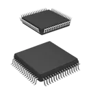
Package information
Special features
Pin descriptions
Pins 1-16
Pins 17-32
Pins 33-48
Pins 49-64 and exposed pad
4) Symbol and footprint cross-check
What matches
Issues flagged
Bottom line
Overall assessment
Most important corrections
Table
| Field | Value |
|---|---|
| MPN | BD34301EKV-E2 |
| Manufacturer | Rohm |
| Description | DAC, Audio 32 b 768kHz DSD, I2C, PCM 64-HTQFP (10x10) #CommonPartsLibrary #IntegratedCircuit #MUS-IC™ |
| Part type | Integrated Circuit |
| Datasheet URL | Present |
| Package from datasheet | HTQFP64BV |
| Package size from datasheet | 12.0 mm x 12.0 mm x 1.0 mm |
| Datasheet pin count | 64 pins + exposed pad |
| Part-project symbol terminals present | 65 terminals total |
A datasheet URL was already set on the part, so step 2 was not needed.
3) Datasheet summary
Device overview
Table
| Item | Summary |
|---|---|
| Part | 32-bit high sound quality stereo audio D/A converter |
| PCM support | 32 kHz to 768 kHz |
| PCM word length | 16-bit to 32-bit |
| DSD support | 2.8224 MHz to 22.5792 MHz |
| Control interface | 2-wire interface, up to 400 kHz |
| Selectable I2C addresses | 38h, 3Ah, 3Ch, 3Eh |
| Audio modes | Stereo (2ch) and Mono (1ch) |
| Filters | Sharp Roll-Off and Slow Roll-Off |
| Typical audio performance | SNR 130 dB, THD+N -115 dB |
Table
| Parameter | Symbol | Rating |
|---|---|---|
| Supply voltage | AVCC | 7.0 V |
| Supply voltage | DVDDIO | 7.0 V |
| Supply voltage | DVDD | 2.1 V |
| Input voltage | Vin | -0.3 V to DVDDIO + 0.3 V |
| Storage temperature | Tstg | -55 °C to +150 °C |
| Maximum junction temperature | Tjmax | 150 °C |
Table
| Parameter | Symbol | Min | Typ | Max |
|---|---|---|---|---|
| Analog supply | AVCC | 4.5 V | 5.0 V | 5.5 V |
| Digital I/O supply | DVDDIO | 3.0 V | 3.3 V | 3.6 V |
| Digital core supply | DVDD | 1.4 V | 1.5 V | 1.6 V |
| Operating temperature | Topr | -25 °C | +25 °C | +85 °C |
Table
| Parameter | Conditions | Typ | Max |
|---|---|---|---|
| AVCC current | PCM, no signal | 30.5 mA | 45.0 mA |
| DVDDIO current | PCM, no signal | 10 µA | 100 µA |
| DVDD current 1 | PCM, no signal | 10 mA | 20 mA |
| DVDD current 2 | PCM, 0 dBFS, 44.1 kHz | 11 mA | 22 mA |
| DVDD current 3 | PCM, 96 kHz | 18 mA | 36 mA |
| DVDD current 4 | PCM, 192 kHz | 17 mA | 34 mA |
| DVDD current 5 | PCM, 384 kHz | 10 mA | 20 mA |
| DVDD current 6 | PCM, 44.1 kHz, max DVDD current setting | 21 mA | 42 mA |
Table
| Parameter | Min | Typ | Max |
|---|---|---|---|
| SNR | 126 dB | 130 dB | - |
| THD+N | - | -115 dB | -100 dB |
| Dynamic range | 126 dB | 130 dB | - |
| Channel gain mismatch | -0.5 dB | 0 dB | +0.5 dB |
| Output center current | 4.6 mA | 5.3 mA | 6.0 mA |
| Peak output current | 8.5 mApp | 9.8 mApp | 11.1 mApp |
| Sampling frequency | 32.0 kHz | 44.1 kHz | 768.0 kHz |
Table
| Parameter | Min | Typ | Max |
|---|---|---|---|
| SNR | 115 dB | 125 dB | - |
| THD+N | - | -113 dB | -103 dB |
| Dynamic range | 107 dB | 120 dB | - |
| Output center current | 4.6 mA | 5.3 mA | 6.0 mA |
| Peak output current | 4.6 mApp | 5.3 mApp | 6.0 mApp |
| DSD clock | 2.8224 MHz | - | 22.5792 MHz |
Table
| Item | Value |
|---|---|
| Package name | HTQFP64BV |
| Package size | 12.0 mm x 12.0 mm x 1.0 mm |
| Ordering code | BD34301EKV-E2 |
| Package code in ordering | EKV = HTQFP64BV |
| Packing spec | E2 = Embossed tape and reel |
| Exposed pad requirement | Connect the EXP-PAD to AGND |
Table
| Feature | Value |
|---|---|
| Series | MUS-ICTM Series |
| FIR filters | 2 kinds |
| Address selection | 4 device addresses |
| Audio controls | LR swap, stereo/mono, polarity inversion |
| Interfaces | PCM I/F, DSD I/F, 2-wire I/F, MCLK |
| Applications | CD/SACD player, DAP, USB-DAC and others |
Table
| Pin | Name | I/O | Function |
|---|---|---|---|
| 1 | RESETB | Input | Reset, L: Reset |
| 2 | DGND1 | - | Digital ground |
| 3 | SDA | I/O | 2-wire data, open-drain in 2-wire operation |
| 4 | SCL | Input | 2-wire clock |
| 5 | ADDR1 | Input | Device address selector 1 |
| 6 | ADDR2 | Input | Device address selector 2 |
| 7 | DVDD1 | - | Digital core power supply 1.5 V |
| 8 | TEST1 | Input | Test pin, datasheet says open |
| 9 | DGND1 | - | Digital ground |
| 10 | TEST2 | Input | Test pin, datasheet says open |
| 11 | DVDDIO1 | - | Digital I/O power supply 3.3 V |
| 12 | BCLK/DSDCLK | Input | PCM bit clock / DSD clock |
| 13 | LRCLK/DSD2 | Input | PCM LR clock / DSD2 data |
| 14 | DIN/DSD1 | Input | PCM serial data / DSD1 data |
| 15 | DGND1 | - | Digital ground |
| 16 | TEST3 | Input | Test pin, datasheet says open |
Table
| Pin | Name | I/O | Function |
|---|---|---|---|
| 17 | DVDD1 | - | Digital core power supply 1.5 V |
| 18 | TEST4 | Input | Test pin, datasheet says open |
| 19 | TEST5 | Input | Test pin, datasheet says open |
| 20 | TEST6 | Input | Test pin, datasheet says open |
| 21 | TEST7 | Input | Test pin, datasheet says open |
| 22 | N.C. | - | No connection, datasheet says open |
| 23 | AGND3_R | - | Right-channel analog ground |
| 24 | N.C. | - | No connection, datasheet says open |
| 25 | AVCC3_R | - | Right-channel analog power 5.0 V |
| 26 | AVCC2_R | - | Right-channel analog power 5.0 V |
| 27 | N.C. | - | No connection, datasheet says open |
| 28 | AGND2_R | - | Right-channel analog ground |
| 29 | IOUT_RN | Output | Right-channel negative output |
| 30 | IOUT_RP | Output | Right-channel positive output |
| 31 | AGND1_R | - | Right-channel analog ground |
| 32 | N.C. | - | No connection, datasheet says open |
Table
| Pin | Name | I/O | Function |
|---|---|---|---|
| 33 | AVCC1_R | - | Right-channel analog power 5.0 V |
| 34 | AVCC_R | - | Right current-segment analog power 5.0 V |
| 35 | AVCC_R | - | Right current-segment analog power 5.0 V |
| 36 | AVCC_R | - | Right current-segment analog power 5.0 V |
| 37 | AVCC_R | - | Right current-segment analog power 5.0 V |
| 38 | VREF_R | Output | External capacitor, recommended 0.1 µF + 100 µF |
| 39 | AGND | - | Analog ground |
| 40 | EXT_RES_R | Output | External resistor, recommended 910 Ω |
| 41 | EXT_RES_L | Output | External resistor, recommended 910 Ω |
| 42 | AVCC | - | Analog power 5.0 V |
| 43 | VREF_L | Output | External capacitor, recommended 0.1 µF + 100 µF |
| 44 | AVCC_L | - | Left current-segment analog power 5.0 V |
| 45 | AVCC_L | - | Left current-segment analog power 5.0 V |
| 46 | AVCC_L | - | Left current-segment analog power 5.0 V |
| 47 | AVCC_L | - | Left current-segment analog power 5.0 V |
| 48 | AVCC1_L | - | Left-channel analog power 5.0 V |
Table
| Pin | Name | I/O | Function |
|---|---|---|---|
| 49 | N.C. | - | No connection, datasheet says open |
| 50 | AGND1_L | - | Left-channel analog ground |
| 51 | IOUT_LP | Output | Left-channel positive output |
| 52 | IOUT_LN | Output | Left-channel negative output |
| 53 | AGND2_L | - | Left-channel analog ground |
| 54 | N.C. | - | No connection, datasheet says open |
| 55 | AVCC2_L | - | Left-channel analog power 5.0 V |
| 56 | AVCC3_L | - | Left-channel analog power 5.0 V |
| 57 | N.C. | - | No connection, datasheet says open |
| 58 | AGND3_L | - | Left-channel analog ground |
| 59 | DGND2 | - | Digital ground for MCLK |
| 60 | MCLK | Input | Master clock |
| 61 | DVDDIO2 | - | Digital I/O power for MCLK 3.3 V |
| 62 | N.C. | - | No connection, datasheet says open |
| 63 | DVDD2 | - | Digital power for MCLK 1.5 V |
| 64 | DVDD1 | - | Digital core power 1.5 V |
| EP | EXP-PAD | - | Connect to AGND |
Table
| Check | Result | Notes |
|---|---|---|
| Pin count | Match | Datasheet shows 64 pins + exposed pad; part project contains 65 terminals/pads |
| Pin numbering | Match | Symbol terminals include pins 1-64 and 65 for exposed pad |
| Pin naming | Match | Signal names in the symbol align with datasheet naming, including duplicated supply names and separate grounds |
| Exposed pad presence | Match | Project includes EP and datasheet requires EXP-PAD |
| Footprint existence | Present | DRC does not report a missing footprint |
Table
| Severity | Issue | Why it matters |
|---|---|---|
| High | The exposed pad EP is present, but I could not verify from the accessible PCB data that it is explicitly tied to AGND in the footprint definition or symbol intent | The datasheet explicitly requires the exposed pad to be connected to AGND. If left floating or mapped incorrectly, this can cause thermal and analog performance problems |
| Medium | All symbol terminals are currently typed as Unspecified in the project data, including pins like SDA, SCL, RESETB, IOUT_LP, and grounds like AGND | This will not change manufacturing output directly, but it weakens ERC and makes integration mistakes more likely |
| Medium | TEST pins TEST1 through TEST7 and N.C. pins such as N.C._1 are present as normal terminals | The datasheet says TEST pins and N.C. pins must be left open. If later connected in a design, that can cause board failure or undefined behavior |
| Medium | Package text in project description says 64-HTQFP (10x10), while the datasheet package is HTQFP64BV, 12.0 mm x 12.0 mm x 1.0 mm | This can cause incorrect part ordering or a wrong footprint selection if someone relies on the description instead of the datasheet |
| Low | I could confirm pad presence but not exact pad geometry, lead pitch, courtyard, or exposed-pad dimensions from the available layout output | A dimensional footprint error could still exist even though the pad count/name mapping looks correct |
Table
| Area | Status |
|---|---|
| Metadata completeness | Good |
| Datasheet availability | Good |
| Pin-map consistency | Good |
| Manufacturing-risk items | Needs review |
Table
| Priority | Recommendation |
|---|---|
| 1 | Ensure EP is mapped and documented as AGND-connected exposed pad |
| 2 | Update the package description to HTQFP64BV, 12.0 mm x 12.0 mm x 1.0 mm |
| 3 | Set proper pin electrical types for SDA, SCL, RESETB, MCLK, outputs, power pins, and grounds |
| 4 | Mark TEST and N.C. pins as intentionally open in the part definition notes/properties |
If you want, I can next produce a pin-by-pin verification matrix for every terminal in the part project.
Pin verification matrix
Check EP mapping
Review package mismatch
Inspect part properties


Welcome 👋
Flux accelerates your PCB design with AI.
Create your account to start using this component and bring your ideas to life.