Linear Voltage Regulator IC Positive Fixed 1 Output 600mA SOT-25 3.3V LDO AP2112K-3.3
The AP2112K-3.3TRG1 is a low dropout (LDO) linear voltage regulator designed to provide a stable 3.3V output from a higher input voltage. It is optimized for low noise, high power supply rejection ratio (PSRR), and low quiescent current, making it suitable for battery-powered and noise-sensitive applications. The device features current limiting and thermal shutdown protection, ensuring reliable operation under fault conditions. It is commonly used in portable electronics, RF modules, microcontroller power supplies, and other low-power systems.
Key Features
Fixed output voltage: 3.3V
Output current: up to 600 mA
Low dropout voltage: ~250 mV at 300 mA load
High PSRR: up to 70 dB at 1 kHz
Low quiescent current: typically 55 µA
Stable with low ESR ceramic capacitors
Built-in overcurrent protection
Thermal shutdown protection
Fast transient response
Absolute Maximum Ratings
Input Voltage (VIN): up to 6.5 V
Output Current: Internally limited
Operating Junction Temperature: -40°C to +125°C
Storage Temperature: -65°C to +150°C
Electrical Characteristics (Typical values unless otherwise specified)
Output Voltage Accuracy: ±2%
Dropout Voltage:
250 mV @ 300 mA
400 mV @ 600 mA
Line Regulation: 0.05%/V
Load Regulation: 0.2%
Quiescent Current: 55 µA
Shutdown Current: <1 µA
PSRR:
70 dB @ 1 kHz
45 dB @ 10 kHz
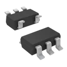
Pin Configuration (SOT-23-5 / SC-70-5)
VIN – Input voltage
GND – Ground
EN – Enable (active high)
NC – No connection
VOUT – Regulated output (3.3V)
Package Information
Package Type: SOT-23-5 (TRG1 suffix indicates tape & reel)
Mounting: Surface mount
Small footprint suitable for compact PCB layouts
Typical Applications
Battery-powered devices
Wireless modules (Wi-Fi, Bluetooth, RF)
Microcontroller and FPGA power supplies
Portable consumer electronics
Sensor and analog circuits requiring low noise
Compliance & Reliability
RoHS compliant
Lead-free package
Designed for high reliability and long operational life