Part Project Review and Validation
2:05
Assess.
Analyzing the schematic.
Analyzing the PCB layout.
Reviewing the bill of materials.
Looking for "part summary description package pin count and ordering information" in ADG2128BCPZ-HS-RL7.pdf
Looking for "absolute maximum ratings supply voltage analog input range digital input voltage current temperature" in ADG2128BCPZ-HS-RL7.pdf
Looking for "recommended operating conditions supply voltage VL VDD VSS analog signal range temperature" in ADG2128BCPZ-HS-RL7.pdf
Looking for "electrical characteristics on resistance leakage capacitance bandwidth THD crosstalk I2C timing" in ADG2128BCPZ-HS-RL7.pdf
Looking for "pin configuration and function descriptions for all pins including EP NC reset SDA SCL A0 A1 A2 VL VDD VSS X0 to X11 Y0 to Y7" in ADG2128BCPZ-HS-RL7.pdf
Looking for "package information dimensions LFCSP 32 lead exposed pad" in ADG2128BCPZ-HS-RL7.pdf
Looking for "features applications special features i2c serial interface reset address pins" in ADG2128BCPZ-HS-RL7.pdf
Analyzing the PCB layout.
Analy.
Assess.
Project and Part Metadata Review
| Field | Value |
|---|---|
| MPN | ADG2128BCPZ-HS-RL7 |
| Manufacturer | Analog Devices |
| Description | Analog Audio/Video 300 MHz 8 x 12 32-Pin LFCSP EP T/R |
| Datasheet URL | Present on project |
| Package in project metadata | LFCSP |
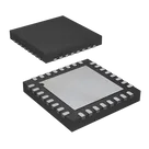
| Datasheet package | 32-Lead LFCSP_WQ, CP-32-7, 5 mm x 5 mm |
| Pin count in schematic | 33 pads/pins total |
| Functional pin count in datasheet | 32 leads + exposed pad |
| Schematic implementation style | One terminal per pin, no internal symbol body |
| Nets defined | None yet |
Schematic Symbol Structure Review
Datasheet Metadata Summary
| Category | Extracted data |
|---|---|
| Device type | I2C-compatible CMOS 8 x 12 unbuffered analog switch array |
| Channels | 96 bidirectional switch channels |
| I2C support | 100 kHz, 400 kHz, 3.4 MHz (-HS version) |
| Bandwidth | Up to 300 MHz |
| On resistance | 35 Ohm max |
| Quiescent current | < 20 uA |
| Logic features | Double-buffered input logic, simultaneous update of multiple switches, readback in standard/fast mode |
| Reset behavior | RESET low opens all switches and clears registers; power-on reset defaults all switches off |
| Addressing | 7-bit slave address, MSBs fixed to 1110, LSBs set by A0, A1, A2 |
| Applications | AV switching, automotive infotainment, CCTV, ultrasound, KVM, telecom, instrumentation, PBX |
Absolute Maximum Ratings
| Parameter | Rating |
|---|---|
| VDD to VSS | 15 V |
| VDD to GND | -0.3 V to +15 V |
| VSS to GND | +0.3 V to -7 V |
| VL to GND | -0.3 V to +7 V |
| Analog inputs | VSS - 0.3 V to VDD + 0.3 V |
| Digital inputs | -0.3 V to VL + 0.3 V or 30 mA, whichever occurs first |
| Continuous current, single input to single output, 10 V on input | 65 mA |
| Continuous current, single input to single output, 1 V on input | 90 mA |
| Continuous current, eight inputs to eight outputs, 10 V on input | 25 mA |
| Operating temperature, B version | -40 C to +85 C |
| Operating temperature, Y version | -40 C to +125 C |
| Storage temperature | -65 C to +150 C |
| Junction temperature | 150 C |
Recommended / Characterized Operating Conditions
| Condition | Value |
|---|---|
| Single-supply characterization | VDD = 12 V ± 10%, VSS = 0 V, VL = 5 V, GND = 0 V |
| Dual-supply characterization | VDD = +5 V ± 10%, VSS = -5 V ± 10%, VL = 5 V, GND = 0 V |
| Analog signal range | VDD - 2 V max |
| Temperature range, B version | -40 C to +85 C |
| Temperature range, Y version | -40 C to +125 C |
Key Electrical Characteristics
| Parameter | Datasheet values |
|---|---|
| On resistance at 12 V / 0 V supplies | 30 Ohm typ / 35-40 Ohm max at VIN = 0 V; 32 Ohm typ / 37-42 Ohm max at VIN = 1.4 V; 45 Ohm typ / 50-57 Ohm max at VIN = 5.4 V |
| On resistance at +5 V / -5 V supplies | 34 Ohm typ / 40-45 Ohm max at VIN = VSS; 50 Ohm typ / 55-65 Ohm max at VIN = 0 V; 66 Ohm typ / 75-85 Ohm max at VIN = 1.4 V |
| Channel leakage | ±0.03 uA typ on/off |
| Capacitance at 12 V / 0 V | COFF 11 pF typ, CON 18.5 pF typ |
| Capacitance at +5 V / -5 V | COFF 6 pF typ, CON 9.5 pF typ |
| -3 dB bandwidth, individual channel | 210 MHz typ at 12 V / 0 V, 300 MHz typ at +5 V / -5 V |
| -3 dB bandwidth, 8 inputs to 1 output | 16.5 MHz typ at 12 V / 0 V, 18 MHz typ at +5 V / -5 V |
| THD + N | 0.04% typ |
| Crosstalk at 5 MHz | Adjacent -63 dB typ / -62 dB typ, nonadjacent -76 dB typ / -79 dB typ |
I2C Timing Highlights
| Parameter | Value |
|---|---|
| fSCL | 100 kHz, 400 kHz, 3.4 MHz with CB = 100 pF max; 1.7 MHz with CB = 400 pF max |
| tHIGH | 4 us, 0.6 us, 60 ns / 120 ns |
| tLOW | 4.7 us, 1.3 us, 160 ns / 320 ns |
| tSU;DAT | 250 ns, 100 ns, 10 ns |
| tHD;DAT | 0 to 3.45 us, 0 to 0.9 us, 0 to 70 ns / 150 ns |
Pin Descriptions
| Pin(s) | Function |
|---|---|
| VSS | Negative supply in dual-supply mode; tie to ground in single-supply mode |
| NC_1, NC_2 | Not connected internally; do not connect |
| X0 to X11 | Analog switch terminals, bidirectional |
| Y0 to Y7 | Analog switch terminals, bidirectional |
| VDD | Positive power supply input |
| VL | Logic power supply input |
| SDA | Bidirectional open-drain data line; external pull-up required |
| SCL | Serial clock input; external pull-up required |
| A0, A1, A2 | Address select inputs |
| ~RESET | Active-low reset; opens all switches and clears registers |
| GND | Ground reference |
| EP | Exposed pad; solder to VSS; recommended for heat dissipation and crosstalk improvement |
Package Dimensions
| Item | Datasheet value |
|---|---|
| Package | 32-Lead LFCSP_WQ (CP-32-7) |
| Body size | 5.10 / 5.00 / 4.90 mm square |
| Pitch | 0.50 mm BSC |
| Package height | 0.80 / 0.75 / 0.70 mm |
| Terminal length | 0.50 / 0.40 / 0.30 mm |
| Lead width | 0.30 / 0.25 / 0.18 mm |
| Exposed pad | 3.25 / 3.10 / 2.95 mm square |
| Coplanarity | 0.08 mm |
Cross-Check: Symbol and Footprint vs Datasheet
| Check item | Result | Risk |
|---|---|---|
| Pin count | Pass - project has 32 leads + exposed pad | Low |
| Pin numbering | Pass - schematic numbering matches datasheet Table 5 | Low |
| NC pins | Pass - NC_1 and NC_2 are correctly present | Low |
| RESET naming | Pass - ~RESET matches active-low RESET function | Low |
| Exposed pad presence | Pass - EP exists as pad 33 | Low |
| Exposed pad electrical requirement | Warning - datasheet says exposed pad is soldered to VSS and recommends soldering to VSS for thermal/crosstalk reasons; project currently has no nets defined | High if left unconnected in a real design |
| Footprint package family | Pass with note - footprint asset name is QFN50P500X500X80-33N-D, while datasheet calls package LFCSP_WQ CP-32-7; dimensions and 33-pad structure align | Medium metadata ambiguity only |
| Footprint pitch | Pass - 0.50 mm matches datasheet | Low |
| Exposed pad size | Pass - footprint center pad 3.25 mm x 3.25 mm matches datasheet max exposed pad size | Low |
| Pad count/orientation | Pass - 8 pads per side plus EP matches package | Low |
| Pull-up requirements on serial pins | Warning - datasheet requires external pull-ups on SDA and SCL; none exist in this part-only project | Not a part-library failure, but important for end-use design |
Issues Most Likely to Matter
| Priority | Finding | Why it matters |
|---|---|---|
| 1 | EP must be tied to VSS in downstream designs | Could cause electrical/thermal/crosstalk problems if omitted |
| 2 | Package metadata is generic LFCSP, while datasheet-specific package is CP-32-7 / LFCSP_WQ | Could increase part-ordering or footprint-selection confusion |
| 3 | No nets are defined in the part project | Prevents validating electrical intent beyond pin mapping |
Bottom Line
To get started, talk to Flux or create a New Document.


Welcome 👋
Flux accelerates your PCB design with AI.
Create your account to start using this component and bring your ideas to life.
