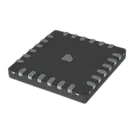
Part Data Review and Validation
Thought for 58 sec
I reviewed the part project end-to-end.
Step 1-2 status
- The part already has a datasheet URL set in project properties: Datasheet
- Because a datasheet URL was already present, there was no need to search the web or update properties.
Table
| Field | Value |
|---|---|
| Description | Single-Ended Input, Quad, Simultaneous Sampling, 16-Bit/14-Bit/12-Bit, SAR ADC |
| Manufacturer | Analog Devices |
| MPN | AD7386-4BCPZ |
| Datasheet | Datasheet |
Table
| Field | Value |
|---|---|
| Family | AD7386-4 / AD7387-4 / AD7388-4 |
| Orderable part | AD7386-4BCPZ |
| Other order codes | AD7386-4BCPZ-RL, AD7386-4BCPZ-RL7 |
| Package | 24-lead LFCSP |
| Package designation | CP-24-25 |
| Body size | 4 mm x 4 mm |
| Package height | 0.55 mm nominal, 0.60 mm max |
| Lead pitch | 0.50 mm BSC |
| Exposed pad | Present, must be connected to GND |
Table
| Feature | Value |
|---|---|
| ADC type | Quad simultaneous-sampling SAR ADC |
| Input type | Single-ended analog inputs |
| Resolution family | 16-bit / 14-bit / 12-bit |
| Max throughput | 4 MSPS |
| Oversampling | On-chip oversampling, 2-bit resolution boost |
| Alert | Out-of-range indicator |
| Reference | 2.5 V internal reference available |
| Logic interface supply | Separate logic supply supports 1.65 V to 3.6 V |
| Temperature range | -40 C to +125 C |
Table
| Parameter | Value |
|---|---|
| VCC | 3.0 V to 3.6 V |
| VLOGIC | 1.65 V to 3.6 V |
| External VREF at REFIO | 2.5 V to 3.3 V |
| Sample rate | Up to 4 MSPS |
| Ambient temperature | -40 C to +125 C |
Table
| Parameter | Rating |
|---|---|
| VCC to GND | -0.3 V to +4 V |
| VLOGIC to GND | -0.3 V to +4 V |
| Analog input to GND | -0.3 V to VREF + 0.3 V, or VCC + 0.3 V |
| Digital input to GND | -0.3 V to VLOGIC + 0.3 V |
| Digital output to GND | -0.3 V to VLOGIC + 0.3 V |
| REFIO to GND | -0.3 V to VCC + 0.3 V |
| Input current except supplies | +-10 mA |
| Operating temperature | -40 C to +125 C |
| Storage temperature | -65 C to +150 C |
| Max junction temperature | 150 C |
| Pb-free reflow | 260 C |
Table
| Parameter | Value |
|---|---|
| Resolution | 16 bits |
| Conversion rate, single-channel pair | 4 MSPS typ |
| Conversion rate, alternating channels | 2 MSPS typ |
| No missing codes | 16 bits |
| DNL | -0.99 / +-0.6 / +1.0 LSB |
| INL, external reference | -7 / +-4 / +7 LSB |
| INL, internal reference | +-3 LSB typ |
| Gain error, external reference 3.3 V | -0.08 / +-0.005 / +0.08 % FS |
| Offset error, external reference | -1 / +-0.07 / +0.1 mV |
| Dynamic range, VREF = 3.3 V | 86 dB typ |
| SNR, VREF = 3.3 V | 84.7 dB typ |
| SNR, VREF = 2.5 V internal | 81.7 dB typ |
| SNR with OSR = 8 | 92 dB typ |
| SFDR | -103 dB typ |
| THD | -100 dB typ |
| SINAD, VREF = 3.3 V | 84.5 dB typ |
| IVCC normal mode | 45 mA typ |
| Total power dissipation | 191 mW typ |
Table
| Pin | Name | Datasheet function |
|---|---|---|
| 1, 5, 14, 16 | GND | Ground reference points |
| 2 | VLOGIC | Logic supply, decouple to GND with 1 uF |
| 3 | REGCAP | Internal regulator decoupling, 1 uF to GND, 1.9 V typ |
| 4 | VCC | Main supply, decouple to GND with 1 uF |
| 6, 7 | AIND1, AIND0 | ADC D analog inputs |
| 8, 9 | AINC1, AINC0 | ADC C analog inputs |
| 10, 11 | AINB1, AINB0 | ADC B analog inputs |
| 12, 13 | AINA1, AINA0 | ADC A analog inputs |
| 15 | REFCAP | Band-gap reference decoupling, 0.1 uF to GND, 2.5 V typ |
| 17 | REFIO | Reference input/output, 2.5 V to 3.3 V external reference allowed, 1 uF decoupling required |
| 18 | CS | Active-low chip select |
| 19 | SDOA | Serial data output A |
| 20 | SDOB | Serial data output B |
| 21 | SDI | Serial data input |
| 22 | SCLK | Serial clock input |
| 23 | SDOC | Serial data output C |
| 24 | SDOD/ALERT | Serial data output D or alert output |
| EPAD | Exposed pad | Must be connected to GND |
Table
| Parameter | Value |
|---|---|
| Package code | CP-24-25 |
| Package style | 24-Lead LFCSP |
| Body | 4.10 / 4.00 / 3.90 mm square |
| Height | 0.60 / 0.55 / 0.50 mm |
| Lead pitch | 0.50 mm BSC |
| Terminal width | 0.30 / 0.25 / 0.20 mm |
| Exposed pad size | 0.60 / 0.50 / 0.40 mm square |
| Coplanarity | 0.08 mm |
Table
| Check | Result | Notes |
|---|---|---|
| MPN | Pass | Project MPN matches datasheet orderable part |
| Package family | Pass | Footprint is a 4 mm x 4 mm, 0.50 mm pitch 24-lead QFN/LFCSP style with center pad |
| Lead count | Pass | Datasheet says 24 leads plus exposed pad; project footprint has 25 pads total |
| Pin numbering | Pass | Symbol pin numbers 1-25 align with footprint pad numbering 1-25 |
| Signal naming | Pass | Signal names align with datasheet names |
| Center pad presence | Pass | Footprint includes pad 25 for the exposed pad |
Table
| Severity | Finding | Why it matters |
|---|---|---|
| Medium | The exposed pad is represented as pin 25 named GND_5 instead of EPAD | Electrically this is likely fine if tied to ground, but it is semantically different from the datasheet and can confuse users, reviews, and reuse of the part |
| Medium | All symbol pins are typed as Unspecified | This will not break fabrication directly, but it weakens ERC and can hide connection mistakes in downstream designs |
| Low | Footprint asset name is generic QFN-style (QFN50P400X400X60-25N-D) while datasheet package is LFCSP CP-24-25 | Geometry appears consistent, so this is not an immediate failure risk, but package naming mismatch can cause ordering/review confusion if someone assumes strict package naming |
| Low | I could not verify paste-mask segmentation, courtyard policy, or assembly land pattern intent beyond the raw footprint definition returned | These details can affect assembly yield on small exposed-pad packages, though no obvious fatal mismatch was visible |
- No obvious fatal symbol-to-footprint mismatch was found.
- The part appears largely consistent with the datasheet for:
- AD7386-4BCPZ
- 24-lead 4 mm x 4 mm LFCSP
- 0.50 mm pitch
- exposed pad present
- The main cleanup item is to rename/document pin 25 as the exposed pad function and assign proper pin electrical types.
Table
| Priority | Recommended correction |
|---|---|
| 1 | Rename or document pad/pin 25 explicitly as EPAD/GND |
| 2 | Set correct pin types for supplies, grounds, inputs, outputs, and digital pins |
| 3 | Optionally align package naming in properties with CP-24-25, 24-lead LFCSP to reduce ambiguity |
If you want, I can next turn this into a concise part QA checklist or a fix list for the part definition.
Create fix list
Run part review
Check footprint details