adrian95 / 760308101214

Loaded

0

0

Files

Schematic

PCB

Log InSign Up

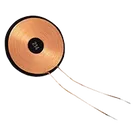
Spiral Coil Design for Ink Stirring

flux

4:44

Following user instructions.

Clarifying tool usage.

Planning the component addition.

Assessing action tool capabilities.

Accessing knowledge base.

Searching for a component.

Searching library for: "691243110004"

Creating search plan for: "691243110004"

Searching.

Searching.

Searching.

Found 51 results.

Searching: "691243110004"

Finished searching for a component.

Searching web for: "Wurth 691243110004 datasheet land pattern"

Found 1 results.

Looking for "PCB layout component view footprint dimensions pad or hole sizes" in 691243110004.pdf

Looking for "recommended PCB layout dimensions land pattern hole diameter pad diameter pitch" in 691243110004.pdf

Looking for "mechanical drawing showing terminal outline and pin spacing" in 691243110004.pdf

Looking for "current rating and wire size range" in 691243110004.pdf

Looking for "hole diameter value symbol Ø numeric value" in 691243110004.pdf

Looking for "drill diameter recommended for PCB layout" in 691243110004.pdf

Looking for "pad diameter annular ring recommendation" in 691243110004.pdf

Looking for "soldering profile reflow wave and PCB hole size notes" in 691243110004.pdf

Searching web for: "691243110004 PCB layout hole diameter pad size"

Found 1 results.

Checking if I can make the changes for you.

Organizing the component addition process.

components to be added to the project

Table


Part NamePurposeManufacturer Part NumberQuantityFootprintDatasheet link
4-position wire-to-board terminal block, 3.5 mm pitch, horizontal, rising cage clampHigh-current edge connection for the stirring coil69124311000413.50 mm pitch, 4-pos, through-holePDF
83 days
yannida

yannida

dimensions
67 days

flux

4:05

Gathering component information.

Confirming component details.

Planning actions for component addition.

Preparing dimensions and adding component.

Accessing knowledge base.

Searching for a component.

Finished searching for a component.

Searching the web.

Found 10 results.

Searching the web.

Looking for "Recommended PCB layout footprint dimensions: hole diameter, pad size, pitch." in 691243110004.pdf

Looking for "Drill plan: plated through hole drill diameter and tolerance." in 691243110004.pdf

Looking for "Mechanical drawing: overall length (L), width (W), height (H) and row-to-edge setback." in 691243110004.pdf

Checking if I can make the changes for you.

Organizing action steps.

components to be added to the project

Table


Part NamePurposeManufacturer Part NumberQuantityFootprintDatasheet link
4-position terminal block, 3.50 mm pitch, horizontal, rising cage clampEdge connector for high-current coil leads69124311000413.50 mm pitch, 4-pos, THTPDF
67 days

​
Sign up to send

To get started, talk to Flux or create a New Document.

Reviews

Documents

    Documents are markdown text files which describe project goals, capture details, or even simulation outputs.

    Assets

    760308101214-thumb.png

    760308101214-thumb.png

    760308101214-thumbThumbnail
    stp

    760308101214.stp

    3D_7603081012143D Model
    kicad_mod

    760308101214.kicad_mod

    FP_760308101214Footprint
    760308101214

    760308101214

    760308101214 Symbol.svgDefault

    760308101214

    760308101214 thumbnail
    1 Coil, 3 Layer 26µH Wireless Charging Coil Receiver 520mOhm Max #CommonPartsLibrary #inductor #coil #Wireless Charging Coils #WE-WPCC

    Properties

    Würth Elektronik

    L

    we-online.com/components/products/download/3d_760308101214+%28rev1%29.pdf

    760308101214

    760308101214

    Inductor

    creativecommons.org/licenses/by/4.0/

    Pricing & Availability

    See prices from popular manufacturers for your project.

    Controls

    Welcome 👋

    Flux accelerates your PCB design with AI.

    Create your account to start using this component and bring your ideas to life.

        Introducing AI Placement!
        AI Placement Demo

        AI-Powered Component Placement

        Let AI place your components intelligently. AI Placement analyzes your schematic and positions components for optimal routing, signal integrity, and board density.

        From Schematic to Layout in Seconds

        Skip the tedious manual placement. AI Placement generates a starting layout you can refine, saving hours of repetitive work on every new design.

        Works With Auto-Layout

        Pair AI Placement with Auto-Layout for a complete AI-driven PCB design flow — from component placement through trace routing, all with one click.

        Try it