Part Review and Datasheet Analysis
1:58
Fetching.
Analyzing the schematic.
Analyzing the PCB layout.
Looking for "Part metadata including description, part number, number of positions, number of rows, pitch, mount orientation, plating, and housing features" in DDEController?Action=showdoc&DocId=Customer+Drawing%7F2209129%7FA%7Fpdf%7FEnglish%7FENG_CD_2209129_A.pdf%7F2209129-1
Looking for "Pin numbering or contact position information" in DDEController?Action=showdoc&DocId=Customer+Drawing%7F2209129%7FA%7Fpdf%7FEnglish%7FENG_CD_2209129_A.pdf%7F2209129-1
Looking for "Recommended operating conditions or application requirements" in DDEController?Action=showdoc&DocId=Customer+Drawing%7F2209129%7FA%7Fpdf%7FEnglish%7FENG_CD_2209129_A.pdf%7F2209129-1
Looking for "Absolute maximum ratings or electrical characteristics" in DDEController?Action=showdoc&DocId=Customer+Drawing%7F2209129%7FA%7Fpdf%7FEnglish%7FENG_CD_2209129_A.pdf%7F2209129-1
Looking for "Package dimensions, PCB footprint dimensions, hole sizes, and mechanical dimensions" in DDEController?Action=showdoc&DocId=Customer+Drawing%7F2209129%7FA%7Fpdf%7FEnglish%7FENG_CD_2209129_A.pdf%7F2209129-1
Looking for "Special features, notes, material, finish, and manufacturing constraints" in DDEController?Action=showdoc&DocId=Customer+Drawing%7F2209129%7FA%7Fpdf%7FEnglish%7FENG_CD_2209129_A.pdf%7F2209129-1
Calcul.
Looking for "Contact numbering pattern, cavity numbers, row and column identification on the drawing" in DDEController?Action=showdoc&DocId=Customer+Drawing%7F2209129%7FA%7Fpdf%7FEnglish%7FENG_CD_2209129_A.pdf%7F2209129-1
Looking for "Any electrical ratings such as current rating, voltage rating, dielectric, insulation resistance, contact resistance" in DDEController?Action=showdoc&DocId=Customer+Drawing%7F2209129%7FA%7Fpdf%7FEnglish%7FENG_CD_2209129_A.pdf%7F2209129-1
Looking for "Recommended PCB layout orientation and pad or drill pattern details for signal and power contacts" in DDEController?Action=showdoc&DocId=Customer+Drawing%7F2209129%7FA%7Fpdf%7FEnglish%7FENG_CD_2209129_A.pdf%7F2209129-1
Looking for "Package or connector outline dimensions and coding key dimensions L1 L2 L3 L4 for part number 2209129-1" in DDEController?Action=showdoc&DocId=Customer+Drawing%7F2209129%7FA%7Fpdf%7FEnglish%7FENG_CD_2209129_A.pdf%7F2209129-1
Project metadata
| Field | Value |
|---|---|
| MPN | 2209129-1 |
| Manufacturer | TE Connectivity |
| Part type | Connector |
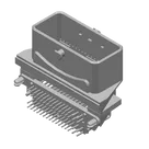
| Description | CMC 64PIN HEADER CONNECTOR ASSEMBLY |
| Mount | PCB / Board Mount |
| Orientation | Horizontal / right-angle style |
| Rows | 4 |
| Positions | 64 |
| Signal vs power positions | 56 signal, 8 power |
| Pitch | 2.5 mm and 3.7 mm |
| Contact types | Pin, Tab |
| Plating | Tin over nickel |
| Housing color | Black |
| Circuit application | Power & Signal |
What exists in the part project
| Area | Observed |
|---|---|
| Schematic symbol | 64 individual terminals using cavity-style names |
| Footprint | 1 footprint with 64 pads, pad names matching the symbol naming style |
| Nets | No nets defined |
| Terminal pin typing | All pins are currently Unspecified |
Electrical / material / general characteristics
| Category | Extracted data |
|---|---|
| Temperature range | -40 °C to 125 °C |
| Max operating temp | 125 °C |
| Recommended PCB thickness | 1.6 mm [.063 in] |
| Contact material | CuZn30 |
| Housing / jointer material | PBT GF30, black |
| Plating, signal pins | Sn (matt) 3.0-5.0 µm solder area, Sn (semi-bright) 0.8-3.3 µm contact area, Ni 1.0-2.5 µm overall |
| Plating, power pins | Sn (matt) 3.0-5.0 µm solder area, Sn (semi-bright) 1.0-3.0 µm contact area, Ni 1.0-2.5 µm overall |
Absolute maximum ratings
| Result | Notes |
|---|---|
| No explicit absolute maximum ratings table found | This document is a customer drawing, not a full electrical datasheet |
Recommended operating conditions
| Parameter | Value |
|---|---|
| Operating temperature | -40 °C to 125 °C |
| PCB thickness | 1.6 ±0.1 mm |
| Intended use | Power & Signal |
Pin descriptions
| Result | Notes |
|---|---|
| No functional per-pin descriptions found | The drawing identifies cavity / circuit numbering, not signal functions |
| Pin naming style | Position-based cavity naming is present on the drawing |
| Implication | Position labels are appropriate, but there are no datasheet-defined signal roles to assign |
Package / mechanical / PCB dimensions
| Feature | Value |
|---|---|
| Overall width | 68.05 ±0.25 mm |
| Body width | 67.2 ±0.25 mm |
| Max height | 53.5 mm max |
| Recommended PCB layout width | 58.8 ±0.15 mm |
| Signal field pitch | 2.5 x 13 = 32.5 mm |
| End offset | 19.85 mm |
| Signal holes | 56x 1.0 mm +0.2/0 |
| Power holes | 8x 1.3 mm +0.2/0 |
| Signal pin size | 0.63 mm |
| Power contact feature | 0.8 ±0.05 mm by 1.5 ±0.05 mm |
| Coding dims for 2209129-1 | L1 16.70 mm, L2 13.90 mm, L3 11.10 mm, L4 8.30 mm |
Special features / notes
| Item | Detail |
|---|---|
| Header type | Fully shrouded |
| Mixed / hybrid | Yes |
| Sealing area | Present |
| Glue area | Present |
| Warping note | Allowed in specified area: -0.2 |
| Flash note | Max flash 0.2 permitted, not in sealing/glue areas |
| Markings | TE logo, assembly date code, month code, cavity numbers, circuit number |
| Compatible mate | 2050859-1 jointer housing |
Passes
| Check | Result |
|---|---|
| Symbol terminal count vs connector positions | Looks consistent |
| Footprint pad count vs connector positions | Looks consistent |
| Symbol naming style vs datasheet cavity-style naming | Looks consistent |
| Connector type vs project metadata | Consistent |
Risks / mismatches flagged
| Severity | Finding | Why it matters |
|---|---|---|
| High | The symbol pins are all typed as Unspecified | This can hide ERC issues and makes the part less robust in real designs |
| Medium | No datasheet-defined per-pin electrical descriptions are present in the symbol | Acceptable for a cavity-defined connector, but users may mis-assign signals without clear cavity documentation |
| High | I could confirm the footprint has 64 pads, but the current layout inspection did not expose numeric pad/drill geometry, so I could not prove the footprint exactly matches the required drill and slot sizes from the drawing | A wrong drill, slot, or pitch would create assembly failure or non-fitting hardware |
| High | The datasheet requires 56 signal holes at 1.0 +0.2/0 mm, 8 power holes at 1.3 +0.2/0 mm, and power-contact features at 0.8 ±0.05 mm x 1.5 ±0.05 mm | Any mismatch here is a manufacturing blocker |
| Medium | The connector is specified for 1.6 ±0.1 mm PCB thickness | If used on a different board thickness, fit and retention may be affected |
| Low | Project metadata uses connector-level description, but the symbol itself is built from generic terminals rather than a rich connector symbol with grouped pin metadata | Not fatal, but weakens usability and reviewability |
Bottom line
| Verdict | Summary |
|---|---|
| Metadata | Good enough for a connector part project |
| Datasheet availability | Present |
| Datasheet completeness | Mechanical/customer-drawing level, not a full electrical datasheet |
| Symbol | Structurally plausible, but under-defined |
| Footprint | Present, but exact drill/slot/pitch compliance is not yet proven from the exposed PCB data |
| Main action item | Numerically verify footprint geometry against the TE drawing before using this part in manufacturing |
To get started, talk to Flux or create a New Document.


Welcome 👋
Flux accelerates your PCB design with AI.
Create your account to start using this component and bring your ideas to life.
