Part Information Review and Analysis
2:18
Review.
Using.
Analyzing the schematic.
Analyzing the PCB layout.
Looking for "Product overview, description, part number, series, connector type, mount style, and package/form factor" in 217176-0001.pdf
Looking for "Number of contacts, pin assignments, terminal layout, signal names, shell and mounting pad details" in 217176-0001.pdf
Looking for "Electrical characteristics including current rating, voltage rating, contact resistance, insulation resistance, dielectric withstanding voltage, temperature range" in 217176-0001.pdf
Looking for "Absolute maximum ratings or maximum electrical and mechanical ratings" in 217176-0001.pdf
Looking for "Recommended operating conditions and environmental specifications" in 217176-0001.pdf
Looking for "Special features, ingress protection, plating, durability, mating cycles, and compliance information" in 217176-0001.pdf
Looking for "Mechanical drawing, package dimensions, recommended PCB layout, land pattern, pad dimensions, and keepout recommendations" in 217176-0001.pdf
Looking for "Overall mechanical dimensions of the connector body including width, depth, height, shell dimensions, and panel cutout dimensions if available" in 217176-0001.pdf
Looking for "Recommended PCB land pattern dimensions including signal pad widths, lengths, positions, shell pad drill sizes, locator hole sizes, and tolerances" in 217176-0001.pdf
Looking for "Terminal numbering and contact names for the 6 circuits, including whether pins are duplicated USB2.0 Type-C contacts" in 217176-0001.pdf
Looking for "Mechanical tolerances and material specifications for shell, contacts, housing, and plating thickness" in 217176-0001.pdf
Looking for "Soldering, reflow, and recommended PCB assembly notes" in 217176-0001.pdf
Looking for "Any tables or notes for contact resistance, insulation resistance, dielectric withstanding voltage, and waterproof sealing performance" in 217176-0001.pdf
Considering.
Part metadata
| Field | Result |
|---|---|
| MPN | 217176-0001 |
| Manufacturer | Molex |
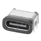
| Description | USB Type-C receptacle, right-angle, surface-mount, top-mount, waterproof IPx5, 6 circuits, gold plating |
| Project description | USB Connectors Top-Mnt SMT IPx5 6Ckt Type C Rec. |
| Mount | Surface Mount |
| Part type | Connector |
| Designator prefix | J |
| Datasheet URL present | Yes |
| Datasheet URL |
Schematic symbol currently implemented
| Symbol terminal | Current name/type in project |
|---|---|
| C1 | Terminal, pin type Unspecified |
| C2 | Terminal, pin type Unspecified |
| C3 | Terminal, pin type Unspecified |
| C4 | Terminal, pin type Unspecified |
| C5 | Terminal, pin type Unspecified |
| C6 | Terminal, pin type Unspecified |
| MP1 | Terminal, pin type Unspecified |
| MP2 | Terminal, pin type Unspecified |
| MP3 | Terminal, pin type Unspecified |
| MP4 | Terminal, pin type Unspecified |
Footprint currently implemented
| Item | Result |
|---|---|
| Footprint asset | 2171760001.kicad_mod |
| 3D model | 217176-0001.stp |
| Electrical/contact pads | 6 SMT pads |
| Shield/mechanical plated holes | 4 plated through-hole pads |
| Non-plated locator holes | 2 NPTH holes |
| Total copper-connected pads mapped to symbol | 10 |
Pad geometry found in footprint
| Pad | Geometry |
|---|---|
| C1 | SMT rect, center (-2.750, -3.74), size 0.800 x 1.670 mm |
| C2 | SMT rect, center (-1.520, -3.74), size 0.760 x 1.670 mm |
| C3 | SMT rect, center (-0.500, -3.74), size 0.700 x 1.670 mm |
| C4 | SMT rect, center (0.500, -3.74), size 0.700 x 1.670 mm |
| C5 | SMT rect, center (1.520, -3.74), size 0.760 x 1.670 mm |
| C6 | SMT rect, center (2.750, -3.74), size 0.800 x 1.670 mm |
| MP1 | PTH circle, center (-4.895, -1.975), pad 2.250 mm, drill 1.5 mm |
| MP2 | PTH circle, center (4.895, -1.975), pad 2.250 mm, drill 1.5 mm |
| MP3 | PTH circle, center (-4.895, 1.025), pad 2.250 mm, drill 1.5 mm |
| MP4 | PTH circle, center (4.895, 1.025), pad 2.250 mm, drill 1.5 mm |
| MP5 | NPTH circle, center (-3.250, -1.875), drill 0.95 mm |
| MP6 | NPTH circle, center (3.250, -1.875), drill 0.95 mm |
Extracted metadata from the available PDF
| Category | Extracted data |
|---|---|
| Series | 217176 |
| Connector type | USB Type-C receptacle |
| Orientation | Right angle |
| Mounting | Surface mount, top mount |
| Shielding | Full shield, shielded |
| Circuits loaded | 6 |
| Rows | 1 |
| Pitch, mating | 0.50 mm |
| Pitch, termination | 0.50 mm |
| PCB thickness recommended | 0.80 mm |
| Current rating | 1.25 A per contact max |
| Voltage rating | 30 V AC/DC max |
| Operating temperature | -40 to +85 C |
| Waterproof rating | IPx5 |
| Durability | 10000 mating cycles max |
| Contact plating | Gold |
| Minimum mating plating | 0.025 um |
| Contact metal | Copper alloy |
| Housing resin | Liquid crystal polymer |
| Other features | Panel mount, PCB locator, PCB retention, lock to mating part |
Table
| Parameter | Retrieved value |
|---|---|
| Voltage - Maximum | 30 V AC/DC |
| Current - Maximum per Contact | 1.25 A |
| Operating Temperature | -40 to +85 C |
| Durability | 10000 mating cycles max |
| Waterproof rating | IPx5 |
Recommended operating conditions
| Parameter | Retrieved value |
|---|---|
| PCB thickness recommended | 0.80 mm |
| Operating temperature | -40 to +85 C |
| Waterproof rating | IPx5 |
| Termination pitch | 0.50 mm |
So from the available scan, I could confirm count, but not the functional names of C1 through C6.
So I could confirm:
- Right-angle, top-mount USB Type-C receptacle
- 0.50 mm pitch
- Recommended PCB thickness 0.80 mm
Special features
| Feature | Result |
|---|---|
| Waterproof | Yes, IPx5 |
| Shielded | Yes |
| Full shield | Yes |
| Panel mount | Yes |
| PCB locator | Yes |
| PCB retention | Yes |
| Lock to mating part | Yes |
| Packaging | Embossed tape on reel |
What matches
| Check | Result |
|---|---|
| 6 loaded circuits in datasheet vs 6 signal/contact pads in footprint | Matches |
| Shielded connector in datasheet vs 4 shell/mechanical plated anchor pads in footprint | Matches |
| PCB locator in datasheet vs 2 NPTH locator holes in footprint | Matches |
| Surface-mount right-angle top-mount style vs footprint structure | Consistent |
| Presence of STEP model | Good for mechanical review |
For a USB Type-C connector, generic names make it easy to miswire VBUS, CC, D+, D-, or SBU-equivalent contacts if this part gets reused in a design. That can cause:
- incorrect schematic connectivity
- wrong board behavior
- possible board failure depending on how the port is used
Unspecified
Unspecified.This weakens ERC quality and makes it harder to catch misuse of power, shield, and signal contacts.
This is the main unresolved manufacturing/ordering risk.
This is normal if the locator holes are purely mechanical and non-electrical.
If this part is used on thicker boards without confirming compatibility, mechanical fit and connector retention may be affected.
Status
| Area | Verdict |
|---|---|
| Basic metadata completeness | Good |
| Datasheet presence | Good |
| Footprint structure vs connector style | Looks consistent |
| Symbol quality for reusable part | Not adequate yet |
| Manufacturing risk | Moderate |
| Functional pin-mapping confidence | Not fully verified |
To get started, talk to Flux or create a New Document.


Welcome 👋
Flux accelerates your PCB design with AI.
Create your account to start using this component and bring your ideas to life.
