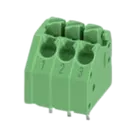
Part Review and Datasheet Verification

Review all available part information (MPN, package, pin count, description, properties). If no datasheet URL is already set, search the web for the official datasheet and update the part's Datasheet property with the URL. Then cross-check the schematic symbol, footprint, and pin descriptions against the datasheet. Summarize key specs and flag any mismatches.
Thought for 6 sec
I’ll review the part metadata and existing symbol/footprint, find and set the official datasheet URL if missing, then cross-check pins and summarize any mismatches.
Worked for 1 min 21 sec
The datasheet URL was already present, so I’m using that official Phoenix Contact PDF for the cross-check. I found the core symbol pin count matches, and I’m recording the detailed review in a project document.
Worked for 56 sec
Review complete. The Datasheet URL was already set to the official Phoenix Contact PDF, so no update was needed.
I found no blocking mismatch for MPN, manufacturer, description, pin count, pin numbering, or basic footprint outline. I flagged sparse pin descriptions/pin type metadata and noted that the returned layout data did not expose drill/pitch values, so the 1.0 mm hole and 3.5 mm pad pitch should be confirmed in the footprint editor.
Detailed report: Part Review: Phoenix Contact 1727016
Fix metadata and verify
Fix pin metadata
Verify footprint dimensions
Run part DRC
Check manufacturing output
Refine this doc
Ask about this doc
Part Review: Phoenix Contact 1727016
Reviewed Part Information
- Manufacturer: Phoenix Contact
- Manufacturer Part Number: 1727016
- Product name / description: PTSA 1,5/ 3-3,5-F BD:1,2,3 printed circuit board terminal block
- Part type: Printed circuit board terminal / PC termination block
- Mounting: Wave soldering / solder PCB terminal
- Positions / potentials / connections: 3 positions, 3 potentials, 3 connections
- Rows: 1
- Pitch: 3.5 mm
- Pin layout: Linear front pinning
- Solder pins per potential: 1
- Datasheet URL property: https://www.phoenixcontact.com/en-us/products/printed-circuit-board-terminal-ptsa-15-3-35-f-bd123-1727016?type=pdf
The Datasheet URL was already set, so no property update was required.
Key Datasheet Specs
- Nominal current: 8 A
- Nominal voltage: 250 V
- Rated voltage: 200 V III/3, 250 V III/2, 400 V II/2
- Rated surge voltage: 2.5 kV
- Nominal conductor cross section: 1.5 mm²
- Conductor range: 0.2 mm² to 1.5 mm² rigid/flexible, AWG 24 to 16
- Ferrule range: 0.25 mm² to 1 mm² without plastic sleeve; 0.25 mm² to 0.5 mm² with plastic sleeve
- Stripping length: 9 mm
- Connection method: Push-in spring connection
- Conductor/PCB connection direction: 45°
- Color: Green
- Material: PA, UL 94 V0
- Operating temperature: -40 °C to +100 °C, depending on current carrying/derating
- Storage/transport temperature: -40 °C to +70 °C
- Assembly temperature: -5 °C to +85 °C
- Width: 12 mm
- Height: 16.7 mm
- Length: 12 mm
- Installed height: 13.1 mm
- Solder pin length: 3.5 mm
- Pin dimensions: 0.4 mm x 0.75 mm
- Recommended PCB hole diameter: 1.0 mm
- Pin spacing: 3.5 mm
- Approvals: cULus recognized; VDE approvals listed in datasheet
Schematic Symbol Cross-Check
Observed schematic symbol implementation:
- Three terminal entries exist, with designators/pin numbers 1, 2, and 3.
- Each terminal has Part Type = Terminal.
- Symbol pin positions are vertically arranged and each terminal has one logical pin.
- Pin Type is currently Unspecified for all three terminals.
Cross-check result:
- Pin count: Matches datasheet: 3 positions / 3 potentials / 3 solder pins.
- Pin numbering: Matches product designation BD:1,2,3 and uses pin numbers 1, 2, 3.
- Terminal function: Acceptable for a terminal block because the datasheet does not assign electrical functions beyond position/potential numbering.
- Pin descriptions: Minimal. The project has no explicit Pin Description such as “Terminal position 1”, “Terminal position 2”, “Terminal position 3”. This is not electrically wrong, but adding descriptions would improve clarity.
- Pin type: “Unspecified” is acceptable for passive terminal positions, but “Passive” would be clearer if the library supports that pin type.
Footprint Cross-Check
Observed PCB footprint implementation from layout inspection:
- Three pad nodes exist: 1, 2, and 3.
- Silkscreen/fab outline indicates an approximately 12 mm x 12 mm body outline, consistent with datasheet body dimensions.
- The layout view shows the footprint outline and reference/value text.
Datasheet footprint requirements:
- 3 through-hole solder pins.
- Linear front pinning.
- Pin spacing: 3.5 mm.
- Recommended PCB hole diameter: 1.0 mm.
- Pin dimensions: 0.4 mm x 0.75 mm.
- Body dimensions: 12 mm width x 12 mm length, height 16.7 mm, installed height 13.1 mm.
Cross-check result:
- Pad count: Matches datasheet: 3 pads.
- Footprint outline: Appears consistent with 12 mm x 12 mm datasheet dimensions.
- Pad numbering: Matches 1, 2, 3.
- Pad geometry / drill diameter: Could not be fully verified from the available layout inspection output because pad hole/drill dimensions were not exposed in the returned data. This should be visually or parametrically confirmed in the footprint editor against the 1.0 mm recommended hole diameter and 3.5 mm pitch.
- Pitch: Not directly exposed in the structured pad data returned. The part metadata and datasheet both specify 3.5 mm; verify the actual pad center-to-center spacing in the footprint editor if manufacturing accuracy is critical.
Mismatches / Issues Flagged
- No blocking datasheet mismatch found for MPN, manufacturer, description, pin count, pin numbering, or basic footprint body outline.
- Pin descriptions are sparse: pins 1, 2, and 3 lack descriptive text beyond their pin number. Suggested descriptions: “Terminal position 1”, “Terminal position 2”, and “Terminal position 3”.
- Pin Type is Unspecified for all terminals. This is acceptable for a connector terminal block, but “Passive” would be clearer if supported.
- Footprint drill/pitch not fully machine-verified from the returned layout data. Datasheet requires 1.0 mm holes and 3.5 mm spacing.
Recommendation
The part is generally consistent with the official Phoenix Contact datasheet. Before release, confirm the actual through-hole drill and pad pitch in the footprint editor, and optionally add clearer pin descriptions/pin type metadata for positions 1 through 3.
Reviewed Part Information
Key Datasheet Specs
Schematic Symbol Cross-Check
Footprint Cross-Check
Mismatches / Issues Flagged
Recommendation