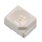
Part Datasheet Analysis and Verification
Thought for 1 min 44 sec
I completed the review for this part project.
1) Available part information
Project metadata
Table
| Field | Value |
|---|---|
| Description | WL-SMTW SMT Mono-color TOP LED, waterclear, 5050 red |
| MPN | 150505RS73300 |
| Manufacturer | Würth |
| Mount | Surface Mount |
| Part type | Optoelectronic Devices |
| Designator prefix | LED |
| Datasheet | Datasheet |
Table
| Symbol terminal | Mapped pin number | Intended polarity from datasheet | Current symbol metadata |
|---|---|---|---|
| K1 | 1 | Cathode | Pin type = Unspecified, pin name undefined |
| A1 | 2 | Anode | Pin type = Unspecified, pin name undefined |
| K2 | 3 | Cathode | Pin type = Unspecified, pin name undefined |
| A2 | 4 | Anode | Pin type = Unspecified, pin name undefined |
| K3 | 5 | Cathode | Pin type = Unspecified, pin name undefined |
| A3 | 6 | Anode | Pin type = Unspecified, pin name undefined |
Table
| Item | Observed |
|---|---|
| Footprint asset | 150505RS73300.kicad_mod |
| 3D model asset | 150505RS73300.stp |
| Pad count | 6 SMD pads |
| Pad numbering | 1 to 6 |
| Pad size in footprint | 1.0 mm x 2.8 mm |
| Pad row span from copper edge to copper edge | 7.2 mm |
| Package body drawing in datasheet | 5.0 mm x 5.0 mm x 1.6 mm |
A datasheet URL was already set, so no update was required.
3) Datasheet scan and extracted metadata
General metadata
Table
| Category | Datasheet value |
|---|---|
| Device type | SMT mono-color TOP LED |
| Lens | Waterclear |
| Chip technology | AlInGaP |
| Emitting color | Red |
| Internal structure | 3 LED chips, ratings specified for all 3 chips in parallel circuit |
| Package size | 5050 |
| Dimensions | 5.0 ± 0.1 mm x 5.0 ± 0.1 mm x 1.6 ± 0.1 mm |
| Terminals | 6 |
| Polarity marking | Cathode polarity mark |
| Viewing angle | 120° typ. |
| Compliance | RoHS compliant, REACh conform/declared, halogen-free |
Table
| Parameter | Conditions | Datasheet value |
|---|---|---|
| Peak wavelength | 60 mA | 630 nm typ. |
| Dominant wavelength | 60 mA | 625 nm typ. |
| Luminous intensity | 60 mA | 2050 min / 2300 typ mcd |
| Forward voltage | 60 mA | 2.0 typ / 2.4 max V |
| Spectral bandwidth | 60 mA | 20 nm typ. |
| Reverse current | 5 V | 10 µA max |
| Viewing angle | 60 mA | 120° typ. |
Table
| Parameter | Conditions | Datasheet value |
|---|---|---|
| Power dissipation | Ambient 25 °C | 156 mW |
| Continuous forward current | Ambient 25 °C | 65 mA |
| Peak forward current | duty/10 @ 1 kHz | 100 mA |
| Reverse voltage | 5 V | |
| ESD threshold, HBM | 2000 V |
Table
| Parameter | Datasheet value |
|---|---|
| Operating temperature | -40 to +85 °C |
| Storage, single parts | -40 to +85 °C |
| Storage, original packaging | < 40 °C, < 90 % RH |
| Moisture sensitivity level | MSL 3 |
| Reflow standard | IPC/JEDEC J-STD-020E |
| Reflow cycles | 2 cycles max. |
| Peak package temperature | Depends on package thickness; for < 1.6 mm, 260 °C |
Table
| Pin | Function |
|---|---|
| 1 | Cathode of chip 1 |
| 2 | Anode of chip 1 |
| 3 | Cathode of chip 2 |
| 4 | Anode of chip 2 |
| 5 | Cathode of chip 3 |
| 6 | Anode of chip 3 |
Table
| Item | Datasheet value |
|---|---|
| Body length | 5.0 ± 0.1 mm |
| Body width | 5.0 ± 0.1 mm |
| Body height | 1.6 ± 0.1 mm |
| Terminal dimensions shown | 0.9 ± 0.2 mm, 0.6 ± 0.2 mm |
| Spacing values shown | 3.3 ± 0.2 mm, 1.05 typ., 3.9 typ. |
| Recommended land pattern values shown | 1.6 mm, 2.8 mm, 7.2 mm, 1.0 mm, 4.0 mm, 0.5 mm |
Table
| Topic | Datasheet note |
|---|---|
| Assembly | Pad pattern is a general recommendation; high-density applications should optimize it |
| Cleaning | Washing agents may damage body, marking, or plating; brushing is not recommended |
| Potting | Shrink/expansion can damage device or sealing |
| Storage time | Use within 12 months of shipment recommended |
| Handling | Pressure on top surface can affect function and reliability |
| ESD | ESD prevention methods required during handling |
Table
| Area | Result | Risk | Details |
|---|---|---|---|
| Pin count | Pass | Low | Symbol exposes 6 pins and footprint has 6 pads, matching the datasheet |
| Pin numbering | Pass | Low | Symbol terminal numbers 1-6 align with footprint terminal IDs 1-6 |
| Pin polarity mapping | Pass | Low | K1, K2, K3 map to cathodes; A1, A2, A3 map to anodes, consistent with the datasheet |
| Footprint pad size | Pass | Low | Footprint uses 1.0 x 2.8 mm pads, matching the datasheet land-pattern values |
| Footprint overall pad span | Pass | Low | Copper span is 7.2 mm, matching the datasheet land-pattern value |
| Package family | Pass | Low | Footprint is clearly built for a 5050 6-pad LED package |
| Symbol pin names | Flag | Medium | The symbol metadata shows pin names as undefined; datasheet functions should be explicit as K1/A1/K2/A2/K3/A3 or C1/A1/C2/A2/C3/A3 in the actual pin properties |
| Symbol pin electrical types | Flag | Medium | All pins are currently Unspecified. For ERC clarity and downstream reuse, these should be set explicitly, typically as passive LED terminals or clearly labeled anode/cathode terminals |
| Datasheet property naming | Minor flag | Low | Project property is Datasheet URL. If your library workflow expects a canonical Datasheet field, consistency may matter for automation, but functionally the URL is present |
- No footprint-to-datasheet mismatch was found that would obviously cause manufacturing failure.
- No pin-count or pad-mapping issue was found that would obviously cause incorrect ordering.
- The main issues are symbol metadata quality, not geometry:
- pin names are not formally defined
- pin types are unspecified
Those two should be cleaned up so this part is safer to reuse and less likely to be miswired later.
@review check ERC
Inspect pad geometry
Find exact pin data