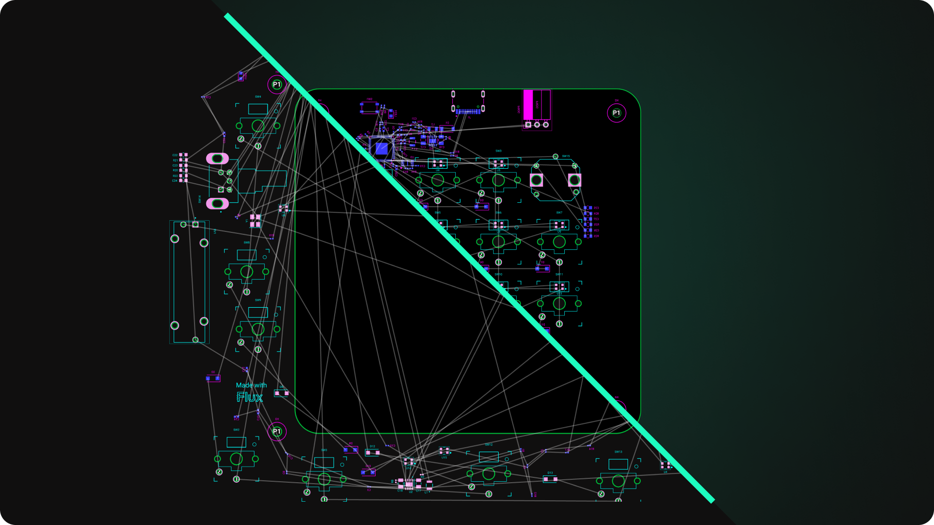
This project is a Pulse Width Modulation (PWM) Controller, built around an LM555 timer IC. It controls a load connected to a MOSFET, with adjustments via a potentiometer, and uses capacitors, resistors and diodes for various functions. #PWM #controller #project #Template #projectTemplate
... show more![[4-layer] OSHPARK Constraints ayg8](https://img-cdn.flux.ai/eyJidWNrZXQiOiJncmF2aXRvbi1lbGVjdHJpYy1zeW1ib2xzIiwia2V5IjoiZG9jdW1lbnRfYXNzZXRzL29zaHBhcmstNGwtMmRkYzI4YzYtOWE0NC00NDM2LTg0ODItOTRlZTVlM2MyMDNjLnBuZyIsImVkaXRzIjp7InJlc2l6ZSI6eyJ3aWR0aCI6NjQsImhlaWdodCI6NjQsImZpdCI6ImNvbnRhaW4iLCJiYWNrZ3JvdW5kIjp7InIiOjAsImciOjAsImIiOjAsImFscGhhIjowfX19LCJvdXRwdXRGb3JtYXQiOiJ3ZWJwIn0=)
Use this template if you're planning to get your board manufactured in OSHPARK. It has the via min/max and trace width constraints already baked as global rules. #project-template #template #manufacturer-design-rules
OSHpark 4-layer stackup specs:
Top overlay or silkscreen: 1 mil thick
Top solder mask or solder resist: 1 mil thick
Top copper: 1.7 mil thick on 1 oz copper
Dielectric: 7.96 mil thick FR408HG 2113
Mid layer 1: 0.68 mil thick on 0.5 oz copper
Dielectric core: 39 mil thick FR408HR
Mid layer 2: 0.68 mil thick on 0.5 oz copper
Dielectric: 7.96 mil thick FR408HG 2113
Bottom copper: 1.7 mil thick on 1 oz copper
Bottom solder mask or solder resist: 1 mil thick
Bottom overlay or silkscreen: 1 mil thick
... show more5 Comments
