Adding PCB Layout for Pins

1:13

Clarifying user intent.

Providing footprint creation instructions.

Exploring help tool usage.

Defining the process for footprints.

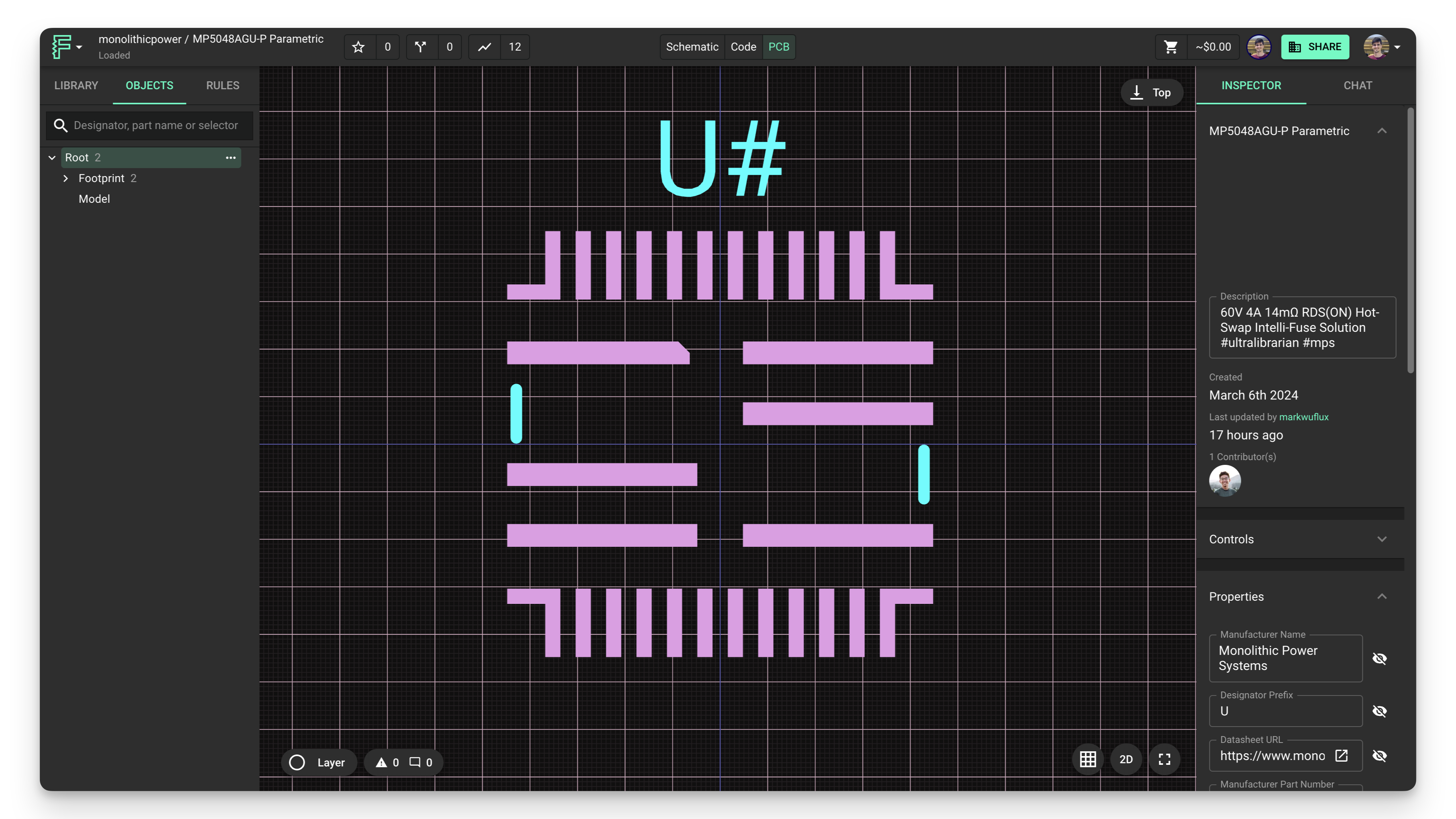
Reading docs about How to create a custom footprint in Flux. Steps to design a 2-pin footprint: open Part/Footprint editor, add pads, set pad size and pitch, set drill (for THT) or pad geometry (for SMD), place courtyard and silkscreen, map footprint pins, save and reuse. Also how to edit an existing footprint..

Calling help for custom footprints.

Here’s what the Flux documentation says about creating custom footprints:
"Create professional footprints that match your team's requirements and design specifications.
Image

Image

Overview
In this tutorial, we'll cover how to work with the PCB Editor to create custom footprints for your components. Whether you're designing a footprint from scratch or modifying an imported footprint, these techniques will help you create accurate, manufacturable component layouts.
Footprints define the physical layout of components on your PCB, including pad sizes, shapes, positions, and silkscreen markings. Creating precise footprints is essential for successful PCB manufacturing and assembly.
Adding Pads
The first step in creating a footprint is adding pads for component pins or leads. Pads are the copper areas where component pins make electrical contact with the PCB."
"Silkscreen markings help identify component orientation and boundaries during assembly. To add silkscreen elements: Adding Silkscreen Lines
Click on the "Objects" tab in the left panel Right-click on the footprint, hover over "Add", and select "Silk line" Add the Shape Start and Shape End rules to the silk line Enter the desired x and y position values for each endpoint
You can also drag endpoints or rotate lines (Right-click → Rotate)
Repeat to create an outline of your component
Adding Text Labels
Click on the "Objects" tab in the left panel Right-click on the footprint, hover over "Add", and select "Text" Add the Content rule to the text node Enter the desired text (e.g., component reference, pin 1 indicator) Position the text appropriately"
Clarify editor entry point
Ask about pad dimensions
Through‑hole vs SMD
Link to component creation
Request step‑by‑step
128 days

Ready.


To get started, talk to Flux or create a New Document.

Documents

    Documents are markdown text files which describe project goals, capture details, or even simulation outputs.

    Assets

    glb

    spst-switch-close

    closed
    glb

    spst-switch-open.glb

    openDefault
    spst-switch-open.svg

    spst-switch-open.svg

    spst-switch-open.svgThumbnail

    SPST Switch

    SPST Switch thumbnail
    A switch that only has a single input and can connect only to one output.

    Properties

    S

    Pricing & Availability

    Distributor

    Qty 1

    Controls

    Switch State