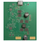
Schematic Design Review
Reviewed: 2026-07-30
Remediation status: Updated 2026-07-30. Confirmed blocking connectivity defects were corrected and the Electrical Rule Checks now return zero open errors or warnings.
Scope: schematic-level electrical connectivity, component support circuits, power/ground distribution, signal integrity intent, and schematic clarity. Findings below are limited to conditions directly present in the current schematic/netlist.
Executive Summary
The schematic contains multiple blocking electrical errors. The highest-priority defects are the TPS25740 VDD supply pin connected directly to GND, both LM5175 differential current-sense pins shorted together, two separate analog-ground networks with no connection to the main GND network, and the USB ESD protector's no-connect pins connected to D+ and D-. These must be corrected before PCB layout or power-up.
Remediation Results
- U1 VDD was removed from GND and connected to the existing 5 V supply/decoupling network.
- U1 AGND/GND/EP and U4 AGND/PGND/PAD now have direct low-impedance GND connectivity. Unsupported 39 kΩ ground-link resistors R23 and R33 were removed.
- D1 is now connected using only its valid protection-channel pins: IOA1/IOA2 on USB_D+ and IOB1/IOB2 on USB_D-. NC pins 3 and 6 are explicitly no-connect.
- U1 GDNS is connected to the Q1/Q2 common-source Kelvin-reference node, named
TPS25740_GDNS_FET_SOURCE.
- J1 SBU1/SBU2 and U4 PGOOD are explicitly marked no-connect because they are unused.
- Critical nets including USB_D+, USB_D-, CC1, CC2, VBUS, and the principal LM5175 switching/gate/sense nets now use functional names.
- U4 ISNS+ and ISNS- remain intentionally shorted because no average-current shunt is implemented; the LM5175 permits this configuration when average-current limiting is disabled. R15 remains dedicated to the CS/CSG cycle-by-cycle current-sense path.
- Fresh Electrical Rule Check result: no matching open errors or warnings, reviewed at 2026-07-30T14:26:49.344Z.
Remaining non-ERC documentation work: capacitor voltage/dielectric ratings and the incorrect U4 datasheet metadata still require cleanup before manufacturing release.
Blocking / Critical Issues
1. TPS25740 U1 VDD is connected to GND
Observed connectivity: The GND net includes U1:VDD, along with U1:GND and U1:EP.
Impact: U1's supply pin is shorted to ground, so the PD controller cannot operate. Depending on the intended VDD source, this can also short that source when populated.
Correction: Disconnect U1:VDD from GND and connect it to the supply rail required by the TPS25740 application circuit. Add/retain the required local VDD bypass capacitor directly between VDD and the appropriate ground.
2. LM5175 U4 ISNS+ and ISNS- are shorted together
Observed connectivity: Net 54 contains only U4:ISNS- and U4:ISNS+.
Impact: The differential input-current sense voltage is forced to zero. Input current monitoring/limiting based on these pins cannot function.
Correction: Route ISNS+ and ISNS- separately to opposite sides of the intended current-sense element using Kelvin connections and the datasheet-recommended input filter. Do not join the two pins at the controller.
3. Analog grounds are isolated from main GND
Observed connectivity:
- Main
GND contains connector ground, power-stage ground, U1 GND/EP, U4 PGND/PAD, and numerous capacitors.
Net 67 separately contains U1:AGND, U3:GND, and associated analog divider/filter returns.Net 36 separately contains U4:AGND and its compensation/configuration returns.- No component or net connection joins
Net 67 or Net 36 to GND.
Impact: U1 and U4 analog references are floating relative to their power grounds. Thresholds, feedback, current sensing, comparator behavior, and converter regulation are therefore undefined.
Correction: Connect each analog-ground network to the intended ground reference exactly as required by the respective IC datasheet, normally at a controlled local star/Kelvin point near the IC exposed pad or quiet ground node. Preserve separate routing intent if desired, but provide an explicit electrical connection to the common ground system.
4. USB ESD protector D1 no-connect pins are connected to D+ and D-
Observed connectivity:
- D+ net (
Net 31) includes D1:NC::6 in addition to D1:IOA1.
- D- net (
Net 30) includes D1:NC::3 in addition to D1:IOB2.
- ERC reports both D1 NC pins as connected no-connect violations.
Impact: The schematic and footprint pin mapping do not match the component definition. PCB copper would be assigned to pins explicitly defined as NC, creating an invalid protection implementation and possible footprint/net assignment errors.
Correction: Remove both NC pins from the USB data nets. Connect D+ and D- only through the valid TPD2E1B06 channel pins according to its pinout, and mark both NC pins as no-connect.
High-Priority Connectivity Issues
5. TPS25740 GDNS is a single-pin net
Observed connectivity: Net 41 contains only U1:GDNS.
Impact: The gate-drive source/sense reference is electrically unconnected. The associated gate-drive function cannot have a defined source reference.
Correction: Connect GDNS to the correct external FET source/Kelvin reference node from the TPS25740 power-path circuit. Verify GDNG and GDNS as a matched gate-drive pair.
6. Unused pins are left floating instead of explicitly marked
Observed ERC findings:
U4:PGOOD floating.J1:SBU1 floating.J1:SBU2 floating.- The schematic contains no no-connect markers.
Impact: These may be intentionally unused, but the current schematic does not document that decision and remains ERC-ambiguous.
Correction: If unused by design, place explicit no-connect markers on U4 PGOOD and J1 SBU1/SBU2. If PGOOD is required by another block, connect it and provide the required pull-up because it is an open-drain status output.
Power and Component-Support Findings
7. Capacitor voltage ratings are unspecified throughout the power path
Observed: The ceramic and electrolytic capacitor components list capacitance but no voltage rating. This includes bulk capacitors connected to converter/input/output and VBUS-related rails, while the design includes 5 V, 12 V, and 20 V operating nodes.
Impact: The schematic does not define whether the capacitors can withstand their connected rail voltages or retain adequate effective capacitance under DC bias. This prevents electrical and BOM verification.
Correction: Add explicit voltage ratings and dielectric/type to every rail capacitor. Use ratings with suitable derating for the actual maximum node voltage and verify effective MLCC capacitance under DC bias. Confirm polarity orientation and voltage rating for C6 and C16.
8. U4 component metadata links to the wrong document
Observed: U4's Datasheet URL points to an LCSC ISO 9001 certification PDF rather than the LM5175 datasheet.
Impact: Pin-function and support-component review cannot be reliably performed from the schematic's linked source, increasing the risk of incorrect wiring or values.
Correction: Replace the U4 datasheet property with the official TI LM5175 datasheet URL and revalidate the converter application circuit against it.
Schematic Clarity and Net-Labeling Issues
9. Most functional nets retain automatic names
Observed: The netlist uses names such as Net 9, Net 31, Net 37, Net 45, and Net 54 for critical rails and signals, even though many portal symbols display functional labels such as VBUS, DVDD, DSG_SW1, DSG_CSP, and FB_20V.
Impact: The authoritative net names do not communicate function. This makes cross-section connectivity difficult to audit and increases the chance of connecting similarly placed portals to the wrong electrical network.
Correction: Rename the actual nets to their functional names. At minimum, name all power rails, USB D+/D-, CC1/CC2, converter switch nodes, gate-drive nets, feedback/sense nets, and enable/control signals. Ensure every repeated portal resolves to exactly one same-named net.
10. Ground naming is inconsistent with actual connectivity
Observed: Symbols visually labeled AGND are represented by separate unnamed nets (Net 67 and Net 36), while the common ground is GND.
Impact: The schematic visually suggests named ground domains but the electrical netlist does not clearly show their relationship, hiding the isolated-ground defects described above.
Correction: Give each intended ground domain an explicit net name and show the exact tie point to GND. If there is no intentional separation, use one canonical GND net throughout.
Positive Observations
- USB CC1 and CC2 each have a direct connection between J1 and U1 and include local capacitors to GND.
- J1's duplicated D+ pins are joined together, and duplicated D- pins are joined together.
- J1 VBUS pins are joined on the same VBUS network.
- U2 has input and output capacitors present; U3 has a local supply bypass path; U4 has local VCC, BIAS, VIN, soft-start, compensation, and bootstrap support components present in the netlist.
- No indicator LEDs are present, so no missing LED current-limiting resistor issue was observed.
Recommended Correction Order
- Fix U1 VDD-to-GND short.
- Separate and correctly route U4 ISNS+ / ISNS-.
- Establish explicit U1 AGND-to-GND and U4 AGND-to-GND connections per datasheet layout intent.
- Correct D1 USB ESD pin mapping and mark its NC pins.
- Connect U1 GDNS to its intended source-reference node.
- Mark intentionally unused U4 PGOOD and J1 SBU pins, or connect them as required.
- Rename functional nets and ground domains.
- Add capacitor voltage/dielectric specifications and correct U4's datasheet link.
- Re-run ERC and perform a focused datasheet-based review of TPS25740 and LM5175 before layout.