Project Buck Converter Overview
1:25
Project Overview
This design implements a compact, high-efficiency buck (step-down) converter using the Texas Instruments TPS54331DR. Its goal is to take a higher input voltage (e.g. 5–28 V) and produce a tightly regulated, adjustable output (0.8 V–VIN) capable of supplying up to 3 A.
This design implements a compact, high-efficiency buck (step-down) converter using the Texas Instruments TPS54331DR. Its goal is to take a higher input voltage (e.g. 5–28 V) and produce a tightly regulated, adjustable output (0.8 V–VIN) capable of supplying up to 3 A.
1. Core Components
| Component | Role |
|---|---|
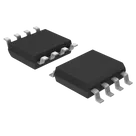
| TPS54331DR | Synchronous buck regulator IC with integrated high-side/low-side MOSFETs, adjustable reference, and internal bootstrap diode. |
| Capacitor | Bulk input decoupling and output filtering to minimize voltage ripple and ensure stability. |
| Inductor | Energy storage element that smooths the switching waveform into a continuous DC output. |
| Resistor | Feedback divider to set the output voltage, plus potential soft-start/pull-down networks. |
2. Functional Blocks & Interactions
-
Input Stage & Decoupling
- Bulk Input Capacitor buffers VIN against switching transients.
- Ensures low impedance at the regulator’s switching frequency (525 kHz).
-
Switching Core (TPS54331DR)
- Drives an internal high-side MOSFET to connect VIN to the PH node.
- On-chip bootstrap network (requires a small Capacitor) for gate drive of the high-side switch.
- Integrated synchronous low-side MOSFET eliminates the need for an external diode, boosting efficiency.
-
Energy Transfer & Filtering
- When the high-side switch is on, current ramps through the external Inductor, storing energy.
- When the switch turns off, the inductor discharges through the low-side MOSFET into the output capacitor, delivering current to the load.
-
Feedback & Regulation Loop
- A resistor divider from VOUT to the VSENSE pin programs the output voltage.
- The internal error amplifier compares VSENSE to its 0.8 V reference and adjusts duty cycle to maintain regulation.
- A small compensation network (Resistor + Capacitor) on the COMP pin ensures loop stability and transient performance.
-
Control & Protection
- EN pin allows digital enable/disable and can be tied to VIN (with a pull-down) for power-on reset.
- SS (soft-start) pin with a capacitor controls inrush current and prevents output overshoot.
- Integrated protections: undervoltage lockout, overcurrent protection, thermal shutdown.
3. Design Choices & Trade-offs
-
Switching Frequency (525 kHz)
- Higher frequency → smaller inductors/caps but increased switching losses and EMI.
- Lower frequency → larger passives but improved efficiency and reduced radiated noise.
-
Synchronous vs. Asynchronous
- Chosen synchronous topology (no external diode) for higher efficiency at light and heavy loads.
- Adds complexity in bootstrap design but avoids diode forward-drop losses.
-
Component Sizing
- Inductor: Rated for ≥3 A with low DCR (3 A, paralleling phases improves ripple current sharing and thermal distribution.
-
EMI Mitigation: Add spread-spectrum modulation or synchronizing multiple converters to reduce interference.
-
Advanced Protection: Integrate input overvoltage protection (e.g., Transient Voltage Suppressor) for harsh environments.
Summary:
This project leverages the high-integration and efficiency of the TPS54331DR to deliver a robust, adjustable 0.8 V–VIN, 3 A buck converter. Optimal passive selection, tight layout practices, and proper loop compensation are key to achieving low noise, high efficiency, and reliable regulation. Future improvements can target digital monitoring, higher currents via multi-phase designs, and advanced EMI controls for demanding applications.
This project leverages the high-integration and efficiency of the TPS54331DR to deliver a robust, adjustable 0.8 V–VIN, 3 A buck converter. Optimal passive selection, tight layout practices, and proper loop compensation are key to achieving low noise, high efficiency, and reliable regulation. Future improvements can target digital monitoring, higher currents via multi-phase designs, and advanced EMI controls for demanding applications.
Inductor selection
Inductance calculation
Compensation parts
Thermal specs
Layout guidance
329 days
To get started, talk to Flux or create a New Document.


Welcome 👋
Flux accelerates your PCB design with AI.
Create your account to start using this component and bring your ideas to life.