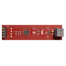
Capacitor Wiring Issues
Thought for 1 min 28 sec
A few things stand out.
- C3 makes sense. TI’s datasheet for U1 explicitly wants a 100 nF supply bypass close to VCC/GND.
- C1 and C2 look like extra bulk decoupling on 3.3 V. They are not inherently wrong, but they are probably more than the transceiver strictly needs. So these were likely added for supply cleanliness, not because the chip absolutely requires all three.
- C4 is the important bus-side one. With R1 and R2, it looks like someone was trying to make split termination. That is a valid CAN technique.
The bigger concern is that the split termination looks wired incorrectly:
But TERM is a 2-way solder jumper, so C4 can connect to one side or the other, not to the true midpoint between R1 and R2. For proper split termination, the capacitor should go to the actual resistor midpoint. As drawn, that network is suspicious and may not behave as intended.
Other possible issues:
- R3 is 10 Ω on the RS pin of U1. TI documents 10 kΩ to 100 kΩ for slope-control mode. With 10 Ω, RS is effectively hard-low, so you get high-speed mode, not real slope control. If the goal was EMI reduction, this is likely wrong.
- C5 and C6 are 68 pF from CANH/CANL to GND. These are not the main capacitor TI calls out for the transceiver. They may have been added as EMI filtering, but they also add line loading and can hurt signal integrity on longer/faster CAN links.
- The ERC warnings are only about branch-point artifacts, so they do not explain a functional CAN problem.
So in short:
Show correct termination
Review RS pin
Assess bus capacitors
Welcome 👋
Flux helps you build PCBs faster with an AI teammate!
Create your account to collaborate, stay updated, fork your own version, and get instant answers from our AI agent.