ARM JTAG/SWD Connector Overview
Thought for 19 sec
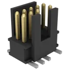
This part is an ARM JTAG/SWD 10-pin 0.05 in / 1.27 mm debug connector footprint/symbol. It is not an active electronic device; it is a compact board connector used to connect an external programmer/debugger to an ARM microcontroller.
Key purpose:
- Provides access to SWD and/or JTAG debug signals.
- Lets tools such as ST-LINK, J-Link, CMSIS-DAP, or other ARM debuggers program firmware, halt/run the CPU, set breakpoints, inspect memory, and sometimes reset the target board.
- The project shows 9 pads for a 10-position connector because the standard ARM Cortex 10-pin header commonly has pin 7 omitted/keyed for polarization.
Typical pin functions:
- VTref, pin 1: Target voltage reference. The debugger senses the target board’s I/O voltage here, e.g. 1.8 V, 3.3 V, etc. It is usually not meant to power the board.
- SWDIO/TMS, pin 2: SWD bidirectional data line, or JTAG TMS.
- GND, pins 3 and 5: Ground reference and return path.
- SWDCLK/TCK, pin 4: SWD clock, or JTAG clock.
- SWO/TDO, pin 6: Optional trace/output signal, or JTAG TDO.
- NC/TDI, pin 8: Usually unused in SWD mode; used as JTAG TDI in full JTAG mode.
- GNDDetect, pin 9: Ground detect / cable detect on some tools.
- RESET, pin 10: Optional target reset control.
How it operates in a circuit:
- The connector simply routes debugger signals between the external debug probe and the target MCU.
- In SWD mode, the essential signals are usually VTref, GND, SWDIO, SWDCLK, and often RESET.
- In JTAG mode, more pins are used: TMS, TCK, TDI, TDO, plus reset/reference/ground.
- It should be placed near the MCU if possible, with short, clean traces for SWDIO and SWDCLK. Pull-ups/pull-downs are usually determined by the MCU vendor’s reference design.
Common applications:
- ARM Cortex-M development boards
- Production programming fixtures
- Firmware debugging
- Factory test access
- Low-volume bring-up and diagnostics
- Embedded products that need a compact debug connector
Family / series context:
- This belongs to the ARM Cortex 10-pin 0.05 in debug connector standard, often called the Cortex Debug connector.
- Compared with the older 20-pin 0.1 in ARM JTAG header, this version is much smaller and better suited for compact PCBs.
- Compared with 6-pin SWD headers, it supports more optional signals such as SWO, JTAG TDI/TDO, GND detect, and reset.
- Compared with Tag-Connect cable pads, it uses a physical mating connector, making repeated debugging easier but consuming more board height and BOM cost.
- Variations include shrouded vs unshrouded headers, vertical vs right-angle, through-hole vs SMD, keyed/missing-pin versions, and smaller board-edge or pogo-pin alternatives.
Notable characteristic: this connector is mainly a debug/programming interface, not a user-facing communication port. It normally carries low-current logic-level signals and should match the target MCU’s I/O voltage through VTref.
Check debug wiring
Map MCU pins
Run ERC/DRC
Find matching header
To get started, talk to Flux or create a New Document.


Welcome 👋
Flux accelerates your PCB design with AI.
Create your account to start using this component and bring your ideas to life.