Chat
Welcome to Flux
Treat Flux like your intern. Tell it what you'd like to build and it'll get to work. You can also ask it questions, brainstorm ideas, and teach it your preferences. Learn More
Explain project
Write a project description
Find schematic issues
Create a test plan
Simulate a circuit
Prepare for Manufacturing
Component Selection Workflow
New Subsystem Wizard
U1
New Comment
3
https://www.electronics-lab.com/wp-content/uploads/2019/04/mpq8626\_tac.jpg

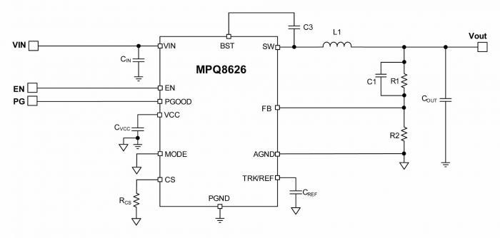
Image
2y
1
give me a rough idea how to accomplish this
@copilot give me a rough idea how to accomplish this
2y
To design a buck converter with an input voltage range of 2.5V-5V, you would need to first select the necessary components. A basic buck converter consists of a transistor switch (MOSFET), diode, inductor, and output capacitor.
Here is a rough step-by-step guide:
-
Start a New Project: In Flux, begin by starting a new project. You can do this by clicking on the "New blank project" option in the menu or by using the ALT+N keyboard shortcut on Windows or ⌥+N on MacOS[1].
-
Add Parts: Use the Flux library to add the necessary components (transistor switch (MOSFET), diode, inductor, and output capacitor) to your project. If the library does not have the component you are looking for, you can create a new part or import one from another tool[2]. Each part has a schematic and potentially a symbol, simulator model, or PCB layout (footprint)[3].
-
Create Circuit Schematic: After adding the components, the next step is to create a schematic of your buck converter. This involves connecting the different components according to the buck converter design. For instance, the MOSFET and diode should be connected on the same node with the diode anode connected to GND. The other side of the MOSFET should connect to the input voltage through an inductor, while the cathode side of the diode connects to the output voltage through a capacitor.
-
Create PCB Layout: Once your circuit schematic is ready, you can proceed to create the PCB layout. This involves defining the footprint for each component and placing them correctly on your PCB. You would also need to route the paths for your circuit. In order to accomplish this, make use of the powerful layout rules and design capabilities provided by Flux[3].
-
Simulation: If desired, you can also simulate your design using the built-in simulator to verify that it behaves as expected[4]. This is especially important for a buck converter where the input to output voltage ratio, duty cycle of the switch and component values need to be verified to ensure they meet the required specifications.
-
Publish to the Library: When your design is final, publish it to the Flux library, so that it is accessible for future use and can be shared with others if desired[5].
Please remember that while the above steps provide a rough guide, the exact process may vary based on the specifics of your design and the tools available in Flux. For more information and specific tutorials on how to perform these steps, please refer to the Flux documentation and additional resources.
Let me know if you need more specific guidance or have any questions about the design or use of Flux.
2y
2
C4
Capacitance
10uF
L1
Inductance
1.5uH
Package
SMD_MAPI-4020
C1
Capacitance
10uF
C3
Capacitance
10uF
H1
C2
Capacitance
1nF
J1
R1
Resistance
10kΩ
P1
No files yet
Reviews
Documents
Documents are markdown text files which describe project goals, capture details, or even simulation outputs.
Assets
No assets added.
Buck Converter

Buck converter , input
voltage range 2.5v-5v
Properties
Properties describe core aspects of the project.
Pricing & Availability
Distributor | Qty 1 |
|---|---|
Mouser | $2.45 |
Controls
Welcome 👋
Flux helps you build PCBs faster with an AI teammate!
Create your account to collaborate, stay updated, fork your own version, and get instant answers from our AI agent.