Guitar Pedal Project Overview
2:19
Analyzing design components.
Structuring component links.
Identifying intents for the project.
Accessing knowledge base.
Reviewing the bill of materials.
Analyzing the schematic.
Setting up queries for knowledge retrieval.
Preparing component and net interactions.
Here’s a clear walkthrough of this Guitar Pedal Template project: what it is, what’s in it, how the pieces connect, and how you can extend it.
Purpose
- A starter “stompbox” template to speed up DIY guitar pedal builds.
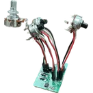
- Provides standardized I/O (input/output 1/4-inch jacks via headers), a 9 V power header, a 3PDT true-bypass wiring header (to an external switch breakout), and a 3-pin potentiometer header.
- PCB size targets a 125B enclosure; design rules match JLCPCB 2-layer defaults.
Core components and roles
Guitar Pedal Template core hardware
Table
| Component | Link | Role |
|---|---|---|
| Power header (2-pin) | J1 | 9 V supply in (P1 = 9 V, P2 = GND). Feeds the pedal circuit and any switch/LED wiring. |
| Input jack header (2-pin) | J2 | Off-board input jack wiring. P1 typically Tip (signal), P2 Sleeve (GND). |
| Output jack header (2-pin) | J3 | Off-board output jack wiring. P1 Tip (signal), P2 Sleeve (GND). |
| 3PDT breakout header (6-pin) | SW1 | Connects to a footswitch breakout to implement true-bypass and optional LED control. |
| Potentiometer header (3-pin) | VR1 | For a board-mounted or wired pot (e.g., gain, tone, level). |
| Circuit ingress portal | CircuitInput | Logical entry point for your effect circuit’s input. |
| Circuit egress portal | CircuitOutput | Logical output from your effect circuit back to the bypass/switch/output wiring. |
| Input jack portal | InputJack | Named net portal tying to input wiring (helps keep the schematic organized). |
| Output jack portal | OutputJack | Named net portal tying to output wiring (organizes schematic). |
How they interact
- Offboard I/O:
- Bypass switching:
- The 3PDT wiring is abstracted by SW1 (01x06 header) intended to mate with an external switch breakout, simplifying chassis wiring.
- The signal path (input -> effect -> output) or direct-through (true-bypass) is achieved by wiring between J2, J3, your effect taps (CircuitInput, CircuitOutput), and the switch header.
- Power:
- 9 V comes in on J1 (P1 = +9 V, P2 = GND per the note). Your effect circuit will derive its rails from here.
- Control:
- VR1 provides a convenient 3-pin interface for a pot (e.g., connect end-to-end across a node and ground, wiper back to the circuit).
Net-level summary (as provided)
- Net 1: SW1:Pin_1 ↔ J3:P1
- Net (J3 - Pin_2): SW1:Pin_3 ↔ J1:P1
- GND: SW1:Pin_4, J2:P2, J1:P2, J3:P2
- Net 7: SW1:Pin_6 ↔ J2:P1
- Net 5: SW1:Pin_5 (currently only this node)
- Net 6: SW1:Pin_2 (currently only this node)
Design, implementation, and functionality
- Schematic organization
- Net portals (InputJack, OutputJack, CircuitInput, CircuitOutput) keep the drawing tidy while maintaining correct electrical connectivity.
- The central work area “Put the circuit here” is where you place your actual effect (e.g., buffer, boost, distortion, filter).
- Offboard wiring minimization
- Using 2-pin headers for jacks and power reduces chassis hand-wiring; the 6-pin header for the 3PDT routes the complex bypass to a small breakout board.
- PCB/layout baseline
- 2-layer stack aimed at low-cost fab (JLC rules).
- Board size is pre-tuned for a 125B enclosure for mechanical fit.
Key technologies, dependencies, and design choices
- “True-bypass” approach via 3PDT
- Pros: preserves tone when bypassed; simple to service.
- Cons: mechanical pops on switching; more wiring than relay/FET soft-bypass solutions.
- Offboard headers vs direct panel-mount
- Pros: faster assembly, clearer serviceability, standardized harnessing.
- Cons: adds connectors and harnesses; potential added series resistance/inductance and failure points if strained.
- Grounding strategy (important for noise)
- Prioritize ground separation over supply separation; return paths dominate noise coupling. Keep noisy/high-current return paths away from sensitive input returns.
- If you later add a switching regulator or digital blocks, manage the ground plane carefully to prevent ground bounce coupling into analog paths via shared returns.
- Mechanical dependency
- Relies on a 3PDT switch breakout and offboard jacks matched to the headers.
- 125B enclosure sizing informs control/jack placement and wiring lengths.
Potential challenges and performance considerations
- Switch pop and thumps
- True-bypass mechanical switching can inject pops if coupling caps are charged or inputs float. Consider adding an input pulldown and providing DC paths for caps to discharge.
- Hum/noise and ground loops
- The instrument, power supply, and chassis grounds can form loops. Keep a clean input ground reference and avoid mixing high-current returns with the input return near the jack.
- Power integrity
- Daisy-chained pedal supplies inject ripple and transients. Add bulk and high-frequency decoupling near where your effect taps power; consider reverse-polarity protection at the 9 V entry.
- ESD and hot-plugging
- Jacks can see ESD events; consider adding series resistors, input clamp diodes, or a small RC for bandwidth-limiting as your effect requires.
- Mechanical stress
- Wires between headers and chassis hardware should be strain-relieved to prevent header solder joint fatigue.
Optimizations and trade-offs
- Bypass architecture
- True-bypass is simple but noisy; a relay- or JFET-based soft-bypass can reduce pops and allow LED control via logic at the cost of complexity and power.
- Grounding and routing
- Use a star ground strategy around the input jack region and isolate high-current or switching returns. Keep the input trace short and away from power traces.
- Input impedance and buffering
- A high-impedance input buffer immediately after the jack can reduce tone loss and noise pickup; it also gives you freedom to place pots elsewhere without loading the pickups.
- Power entry
- Add reverse-polarity protection (series Schottky or ideal diode controller), an input TVS, and an LC/RC filter to suppress supply noise without audible sag.
- LED indication
- Allocate one pole of the switch breakout or a driver transistor for status LED with a current-limiting resistor mounted on the PCB.
Real-world applications
- A baseline for boosts, distortions, fuzzes, EQ/filters, and simple modulation where in/out, one or more pots, a 3PDT switch, and 9 V input are standard.
- Fast prototyping for teaching, DIY kits, or rapid effect iteration.
Areas for improvement, scalability, and future enhancements
- Power and protection
- Add a DC barrel jack footprint and on-board reverse-polarity, surge/ESD protection, and input filtering.
- Optional regulator or charge pump if your effect needs cleaner or alternate rails (e.g., virtual ground or bipolar supply).
- Better documentation on-Board
- Label header pins with functions (Tip/Sleeve, +9 V, GND, LED+, LED-) and add silkscreen arrows for wire dress. Give SW1 a clear pin map for the intended breakout.
- Signal integrity
- Reserve space for input pulldown, input RF filter, output series resistor, and coupling caps as footprints you can stuff as needed.
- Alternative bypass
- Provide a relay/FET soft-bypass subcircuit footprint as an option with the same headers for drop-in swapping.
- Mechanical fit
- Add mounting holes aligned for 125B standoffs; pre-place common control/jack patterns to speed mechanical integration.
- Testability
- Add test pads for 9 V, GND, input, output, and your circuit’s key nodes.
If you want, I can help you:
Audit SW1 pin map
Add pop/noise mitigation
Power entry protection
Check grounding strategy
67 days
To get started, talk to Flux or create a New Document.

Welcome 👋
Flux helps you build PCBs faster with an AI teammate!
Create your account to collaborate, stay updated, fork your own version, and get instant answers from our AI agent.
