Switches
A switch is a device that allows electricity to flow through a circuit by completing or interrupting the connection. It is a common component in electrical and electronic systems and is used in a variety of applications, such as controlling the flow of electricity in a circuit, turning devices on and off, and routing electrical signals. One of the primary use cases for switches is to control the flow of electricity in a circuit. This can be done by manually flipping the switch or by using a control mechanism, such as a timer or a sensor. Another common use for switches is to turn devices on and off. This can be done using a switch that is built into the device or by using a separate switch that is connected to the device. In addition to these basic use cases, switches can also be used to route electrical signals. For example, a switch can be used to route a signal from one device to another or to direct a signal to a specific circuit or component. If you're looking for a wide variety of switches for your projects, flux.ai has the world's largest community-driven public library of them. The library includes footprints, symbols, datasheets, and simulation models for a wide range of switches, making it easy to find the right switch for your needs.
SS510
All details fully confirmed across multiple sources. The SS510 is a 5.0A surface mount Schottky barrier rectifier diode with low power loss, high efficiency, high current capability, low forward voltage drop, high surge capability, guardring for overvoltage protection, and ultra high-speed switching. Here's the complete spec. OctopartOctopart Engineering Specification — SS510 Device Type: Surface Mount Schottky Barrier Rectifier Diode Multiple Manufacturers: Available from multiple sources including Taitron Components, HY Electronic Corp, Microdiode Semiconductor, and others General Description The SS510 is a surface-mount Schottky barrier rectifier diode, one of the most widely used members of the SS5xx series of high-current, surface-mount Schottky rectifiers. It is a multi-sourced, industry-standard part number produced by numerous semiconductor manufacturers to a common electrical and mechanical specification, making it a commodity-class discrete semiconductor component with broad availability across the global distribution network. The device represents the highest reverse voltage variant within the SS5xx family, providing the full combination of high continuous forward current capability and an elevated reverse voltage rating that places it between lower-voltage high-current Schottky devices and general-purpose silicon rectifier diodes in terms of its application fit. Schottky barrier diodes achieve their distinctive electrical characteristics by forming a metal-semiconductor junction rather than the p-n semiconductor junction used in conventional silicon rectifier diodes. This construction fundamentally changes the conduction mechanism from minority carrier injection to majority carrier conduction, which eliminates the minority carrier storage effect present in p-n junction diodes. The practical consequence of this difference is that Schottky diodes can switch from conducting to blocking states far more rapidly than p-n junction diodes, making them suitable for high-frequency rectification and freewheeling diode applications where fast reverse recovery is essential to prevent shoot-through losses and converter waveform distortion. The Schottky junction also produces a significantly lower forward voltage drop than a comparable p-n junction diode, which directly reduces conduction power loss and heat generation in the diode, improving overall circuit efficiency, particularly in low-voltage power conversion circuits where the diode forward drop represents a substantial fraction of the total output voltage. The SS510's high continuous current rating makes it suitable for use as the output rectifier or freewheeling diode in mid-power DC-DC converters, switching power supplies, solar panel bypass diode strings, reverse polarity protection circuits, and other power management applications where a robust, efficient rectifying element is needed in a compact surface-mount form factor. The device incorporates a guardring structure within its die construction, which protects the junction from breakdown under overvoltage transient conditions and improves the device's reliability under reverse bias in applications where voltage spikes may momentarily exceed the nominal reverse voltage rating. Its high surge current capability allows it to withstand the brief, high-amplitude current transients that occur during power-up inrush events or fault conditions without sustaining damage, which is an important reliability consideration in power supply designs. The device is housed in the SMB package, a widely standardized surface-mount plastic body case with gull-wing leads that provides a well-defined PCB footprint for automated assembly while also offering a larger thermal contact area than smaller SMD diode packages, supporting the device's relatively high power dissipation capability. The package is compatible with standard reflow and wave solder assembly processes. Spec Sheet Identification Part Number: SS510 Series: SS5xx Surface Mount Schottky Rectifier Family Manufacturer: Multi-sourced commodity part number Functional Classification Device Type: Schottky barrier rectifier diode Junction Type: Metal-semiconductor Schottky junction Configuration: Single diode Electrical Characteristics Reverse Voltage Rating: High-voltage class for Schottky rectifier, highest in SS5xx series Average Forward Current: High continuous current class Peak Forward Surge Current: High surge capability for inrush and transient events Forward Voltage Drop: Low forward voltage drop, characteristic of Schottky junction Reverse Leakage Current: Low reverse leakage class Junction Capacitance: Low junction capacitance, supporting high-speed switching Switching Performance Recovery Type: Ultra high-speed, negligible reverse recovery time Switching Mechanism: Majority carrier conduction, no minority carrier storage Protection Features Guardring: Integrated guardring for overvoltage protection and junction ruggedness Thermal Characteristics Operating Junction Temperature Range: Extended range, standard high-reliability diode class Storage Temperature Range: Matches operating junction temperature limits Thermal Resistance, Junction to Lead: Defined per package specification Thermal Resistance, Junction to Ambient: Defined per PCB copper pad area Package & Mechanical Package Type: SMB (DO-214AA) Mounting Method: Surface mount technology (SMT) Polarity Marking: Cathode band marked on body per standard convention Target Applications Output rectification in DC-DC switching converters Freewheeling diodes in inductive switching circuits Reverse polarity protection Low-voltage power supply rectification Solar panel bypass diodes Battery charging circuits Environmental & Qualification RoHS Compliance: Yes, lead-free per standard multi-source specifications Packaging Supply Format: Tape-and-reel, per manufacturer standard packaging #SS510 #SchottkyDiode #SchottkyRectifier #SurfaceMountDiode #SMBDiode #DO214AA #PowerRectifier #FreewheelDiode #LowForwardVoltage #HighSpeedSwitching #PowerElectronics #DCDCConverter #PowerSupply #ReversePolarity #DiscreteComponent #SemiconductorDiode #EngineeringSpec #ComponentLibrary #CommonPartsLibrary #RoHSCompliant #CommodityPart
33 Uses0 Stars158301227
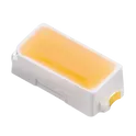
LED Lighting WL-SWTP White, Warm 2700K 3V 20mA 120° 1206 (3216 Metric) The 158301227 is a surface-mount white LED manufactured by Würth Elektronik, belonging to the WL-SWTP series of top-view PLCC-packaged light-emitting diodes designed for general illumination, backlighting, and signal indication applications in compact electronics. It is built on a gallium nitride semiconductor chip, the standard chip technology used in high-efficiency white LED production, which achieves white light emission by combining a blue GaN die with a phosphor conversion layer that down-converts a portion of the blue photons into broader-spectrum yellow light, with the combined blue and yellow output perceived by the human eye as white light. This particular variant is characterized by a warm white Sunrise color temperature, placing it in the lowest color temperature tier of the WL-SWTP family. Warm white light at this color temperature produces a yellowish, incandescent-like appearance that is widely preferred in residential, hospitality, and ambient lighting applications where a soft, comfortable visual environment is desired. This makes the device a natural fit for LED-based replacements for incandescent and halogen light sources in T5 and T8 fluorescent tube form factor products, as well as indoor display backlights, decorative architectural lighting, and other applications where a warm light quality is specified or preferred by end users. The WL-SWTP series features fast switching, no infrared radiation, high color rendering index, slim and miniature size, low power consumption, suitability for all SMT assembly methods, a top-view emission direction, and a wide viewing angle. The high color rendering index characteristic of this device means that objects illuminated by it appear with colors close to how they would look under natural daylight illumination, which is an important quality metric in retail, museum, medical examination, and other environments where accurate color representation enhances user experience or functional accuracy. Texas Instruments The PLCC package style used in this device is a molded plastic leaded chip carrier format that provides a well-defined, mechanically stable footprint for surface-mount assembly, with the optical emitting surface oriented perpendicular to the PCB plane in the top-view configuration. This top-view orientation makes the device suitable for direct illumination of surfaces positioned above the PCB, such as diffusers, light guides, or display panels mounted parallel to the LED board. The compact 3014 package footprint allows high-density LED arrays to be assembled on narrow PCB strips or modules, which is typical in LED tube light and edge-lit backlight designs. The device is supplied on tape-and-reel packaging suitable for automated high-speed pick-and-place assembly at production volumes. Spec Sheet Identification Part Number: 158301227 Series: WL-SWTP — SMD White Top View PLCC LED Manufacturer: Würth Elektronik GmbH & Co. KG Functional Classification Device Type: Surface-mount white LED Chip Technology: Gallium Nitride (GaN) with phosphor conversion Emission Type: White light via blue die plus phosphor down-conversion View Direction: Top view — perpendicular to PCB surface Optical Characteristics Emitting Color: Sunrise warm white Color Temperature: Warm white class, lowest CCT tier in WL-SWTP family Color Rendering Index: High CRI class, suitable for color-critical applications Viewing Angle: Wide angle, broad spatial distribution Infrared Radiation: None — no IR emission Electrical Characteristics Operating Current: Standard signal LED drive current class Forward Voltage: Standard GaN white LED forward voltage class Switching Speed: Fast switching capable Thermal Characteristics Thermal Resistance, Junction to Solder Point: Defined per series specification Maximum LED Junction Temperature: Rated to elevated junction temperature class Package & Mechanical Package Type: PLCC (Plastic Leaded Chip Carrier), PLCC-2 style Package Size: 3014 SMD footprint Mounting Method: Surface mount technology (SMT) Assembly Compatibility: Suitable for all standard SMT assembly methods including reflow soldering Target Applications Signal indication and pilot lights Indoor display backlighting General illumination and commercial lighting Replacement for PLCC 3528 devices in T8 and T5 LED tube designs Architectural and ambient lighting systems Environmental & Qualification RoHS Compliance: Yes REACH Compliance: Yes Packaging Supply Format: Tape-and-reel Standard Reel Quantity: Standard volume reel per Würth packaging convention #WuerthElektronik #WuerthElectronic #WLSWTP #WhiteLED #WarmWhiteLED #SunriseLED #PLCCLED #SMDLed #3014LED #TopViewLED #GaNLED #HighCRI #LEDBacklight #GeneralIllumination #IndoorLighting #SignalLED #LightingDesign #OptoelectronicComponent #EngineeringSpec #ComponentLibrary #CommonPartsLibrary #RoHSCompliant #REACHCompliant
75 Uses0 StarsIXTL2N470
N-Channel 4700 V 2A (Tc) 220W (Tc) Through Hole ISOPLUSi5-Pak™ Full picture confirmed from IXYS/Littelfuse datasheet sources — N-channel MOSFET, unipolar, ultra-high voltage class, housed in the ISOPLUS i5-Pak package. Here's the complete spec. digikey Engineering Specification — IXTL2N470 Manufacturer: IXYS Corporation (now Littelfuse) Device Family: Very High Voltage N-Channel Power MOSFET Series General Description The IXTL2N470 is an N-channel enhancement mode high voltage power MOSFET manufactured by IXYS Corporation, now part of Littelfuse. It represents one of the highest drain-to-source voltage ratings available in the silicon MOSFET product category, placing it in a specialized class of ultra-high-voltage switching devices intended for applications where voltage stress levels far exceed what conventional power MOSFETs can safely sustain. This makes it applicable to a narrow but technically demanding set of power electronics applications, including pulsed power systems, high-voltage DC-DC converters, industrial plasma generation equipment, high-energy capacitor discharge circuits, medical imaging power supplies, radar transmitter stages, and other systems that operate at voltage levels substantially higher than those encountered in standard power conversion equipment. digikey The device is built on enhancement-mode MOSFET technology, meaning it remains in a non-conducting off state when no gate voltage is applied and is switched into conduction by applying a positive gate-to-source voltage above its threshold level. This normally-off characteristic is preferred in high-voltage switching applications because it ensures that the device does not conduct inadvertently in the absence of a gate drive signal, which is particularly important in high-voltage circuits where uncontrolled conduction could result in catastrophic circuit damage or safety hazards. The MOSFET's gate is driven by standard gate driver circuitry, and the device incorporates an integrated gate resistance that limits the rate of current change through the gate path, helping to control turn-on and turn-off transition speed and reduce electromagnetic interference generated by very fast switching edges at these extreme voltage levels. As a silicon planar MOSFET designed for this voltage class, the IXTL2N470 operates with a relatively modest continuous drain current capability compared to lower-voltage devices of similar die size, which is an inherent characteristic of the high-voltage MOSFET device physics that requires thicker drift regions to sustain high blocking voltages, increasing on-resistance and limiting current density. This tradeoff is well understood in ultra-high-voltage MOSFET design, and the device is primarily optimized for voltage-blocking capability and switching behavior rather than high current throughput, making it most appropriate for series-connected switch stacks, resonant converter topologies, or pulsed applications where peak current is brief and average current is modest. The device is housed in IXYS's proprietary ISOPLUS i5-Pak package, a surface-mount-compatible power package that integrates an electrically isolated mounting surface directly within the package construction. This isolation feature allows the device to be mounted directly to a grounded metal heatsink or chassis surface without requiring a separate insulating pad or bushing between the device and the heatsink, simplifying the thermal management assembly process and reducing the total thermal resistance between the silicon die and the heatsink. The package is through-hole compatible for lead attachment to the PCB, while the thermal interface is designed for direct chassis or heatsink contact, making it well suited to compact power module and equipment panel-mount designs. Spec Sheet Identification Part Number: IXTL2N470 Device Family: Very High Voltage N-Channel Standard Power MOSFET Manufacturer: IXYS Corporation (now Littelfuse) Functional Classification Device Type: Power MOSFET Channel Type: N-channel Operating Mode: Enhancement mode (normally off) Technology: Silicon planar high-voltage MOSFET Electrical Characteristics Drain-to-Source Voltage Rating: Ultra-high voltage class, among the highest available in silicon MOSFET technology Drain Current Rating: Low continuous current class, consistent with ultra-high-voltage MOSFET physics Power Dissipation: High power dissipation class for its current rating, reflecting package thermal capability On-Resistance: Relatively high on-resistance, inherent to ultra-high-voltage MOSFET drift region design Gate Threshold: Standard enhancement-mode positive gate threshold voltage Integrated Gate Resistance: Built-in gate resistance for switching transition control and EMI reduction Input Capacitance: Moderate-to-high input capacitance class Reverse Transfer Capacitance: Low reverse transfer capacitance class Switching Characteristics Turn-On Delay: Defined turn-on delay time Rise Time: Defined output voltage rise time Turn-Off Delay: Defined turn-off delay time Fall Time: Defined output voltage fall time Thermal Characteristics Junction-to-Case Thermal Resistance: Defined by package construction and isolated mounting interface Operating Junction Temperature: Standard high-temperature silicon MOSFET class Mechanical & Package Package Type: ISOPLUS i5-Pak (proprietary IXYS isolated surface-mount power package) Isolation Feature: Electrically isolated mounting base integrated within package — no external insulator required for heatsink mounting Mounting Method: Through-hole PCB pin termination with isolated bottom thermal contact Environmental & Qualification RoHS Compliance: Yes Lifecycle Status: Active, available through Littelfuse and authorized distributors Target Applications Application Domains: Pulsed power systems, high-voltage DC-DC converters, plasma generation equipment, medical imaging power supplies, radar transmitter stages, capacitor discharge circuits, high-voltage series switch stacks #IXTL2N470 #IXYS #Littelfuse #HighVoltageMOSFET #UltraHighVoltageMOSFET #NChannelMOSFET #PowerMOSFET #EnhancementMode #ISOPLUSi5Pak #PulsedPower #HighVoltagePower #PowerElectronics #SwitchingDevice #PlasmaEquipment #MedicalPowerSupply #IndustrialPower #SemiconductorIC #DiscreteSemiconductor #EngineeringSpec #ComponentLibrary #CommonPartsLibrary #RoHSCompliant
1 Uses0 StarsBSC040N10NS5ATMA1
N-Channel 100 V 100A (Tc) 2.5W (Ta), 139W (Tc) Surface Mount PG-TDSON-8-7 BSC040N10NS5ATMA1 is a high-performance 100V N-Channel Power MOSFET from Infineon's OptiMOS™ 5 family. It is designed for high-efficiency switching applications such as switched-mode power supplies (SMPS), synchronous rectification, DC-DC converters, motor drives, battery-powered systems, and industrial power management. The device features extremely low on-resistance, high current capability, and excellent thermal performance, making it suitable for demanding power conversion applications. Key Features N-Channel Enhancement Mode MOSFET 100V Drain-to-Source Voltage (VDS) Ultra-low RDS(on): 4.0 mΩ max @ VGS = 10V Continuous Drain Current up to 100A (package limited) Optimized for high-performance SMPS and synchronous rectification Low gate charge for improved switching efficiency 100% avalanche tested for enhanced robustness Superior thermal resistance and power dissipation Wide operating junction temperature range: -55°C to +150°C RoHS compliant and halogen-free Compact PG-TDSON-8 / SuperSO8 package for high power density designs Typical Applications DC-DC Converters Synchronous Rectifiers Motor Control Battery Management Systems (BMS) Telecom and Industrial Power Supplies Solar Power Systems High-Current Switching Circuits #Infineon #OptiMOS5 #MOSFET #NChannelMOSFET #PowerMOSFET #100V #LowRDSon #SMPS #DCDCConverter #MotorDrive #PowerElectronics #IndustrialElectronics #BSC040N10NS5ATMA1 #HighEfficiency #SynchronousRectification
465 Uses0 Stars