Memory
A memory IC, or integrated circuit, is a type of electronic device that stores and retrieves data. It is used in a wide range of electronic devices, including computers, smartphones, and other electronic devices. Memory ICs come in a variety of types, including DRAM, SRAM, and Flash memory, and are used for different purposes depending on the device and application. One of the primary use cases for memory ICs is in computer systems, where they are used to store data and instructions that are accessed by the processor. Memory ICs are also used in a variety of other electronic devices, such as digital cameras, MP3 players, and mobile phones, to store data and enable various functions. Flux.ai has the world's largest community-driven public library of memory ICs, with a wide variety of footprints, symbols, datasheets, and simulation models available. This extensive library allows users to easily access and use memory ICs in their projects, making it an invaluable resource for engineers and developers.
ADXL345BCCZ-RL
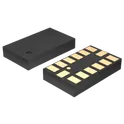
Accelerometer X, Y, Z Axis ±2g, 4g, 8g, 16g 0.05Hz ~ 1.6kHz 14-LGA (3x5) The ADXL345 is a small, thin, ultralow power, 3-axis accelerometer with high resolution (13-bit) measurement at up to ±16 g. Digital output data is formatted as 16-bit twos complement and is accessible through either a SPI (3- or 4-wire) or I2C digital interface. The ADXL345 is well suited for mobile device applications. It measures the static acceleration of gravity in tilt-sensing applications, as well as dynamic acceleration resulting from motion or shock. Its high resolution (3.9 mg/LSB) enables measurement of inclination changes less than 1.0°. Several special sensing functions are provided. Activity and inactivity sensing detect the presence or lack of motion by comparing the acceleration on any axis with user-set thresholds. Tap sensing detects single and double taps in any direction. Free-fall sensing detects if the device is falling. These functions can be mapped individually to either of two interrupt output pins. An integrated memory management system with a 32-level first in, first out (FIFO) buffer can be used to store data to minimize host processor activity and lower overall system power consumption. Low power modes enable intelligent motion-based power management with threshold sensing and active acceleration measurement at extremely low power dissipation. The ADXL345 is supplied in a small, thin, 3 mm × 5 mm × 1 mm, 14-lead, plastic package. ► Ultralow power: as low as 23 µA in measurement mode and 0.1 µA in standby mode at VS = 2.5 V (typical) ► Power consumption scales automatically with bandwidth ► User-selectable resolution ► Fixed 10-bit resolution ► Full resolution, where resolution increases with g range, up to 13-bit resolution at ±16 g (maintaining 4 mg/LSB scale factor in all g ranges) ► Embedded memory management system with FIFO technology minimizes host processor load ► Single tap/double tap detection ► Activity/inactivity monitoring ► Free-fall detection ► Supply voltage range: 2.0 V to 3.6 V ► I/O voltage range: 1.7 V to VS ► SPI (3- and 4-wire) and I2C digital interfaces ► Flexible interrupt modes mappable to either interrupt pin ► Measurement ranges selectable via serial command ► Bandwidth selectable via serial command ► Wide temperature range (−40°C to +85°C) ► 10,000 g shock survival ► Pb free/RoHS compliant #commonpartslibrary #sensor #transducer #accelerometer
203 Uses2 StarsPIC16F877A-I/P
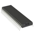
PIC PIC® 16F Microcontroller IC 8-Bit 20MHz 14KB (8K x 14) FLASH 40-PDIP The PIC16F877A-I/P is a high-performance 8-bit microcontroller from Microchip Technology, based on a Harvard architecture with separate program and data memory buses. It is designed for a wide range of embedded applications requiring reliable processing, multiple communication interfaces, and analog capability. The device integrates Flash program memory, EEPROM data storage, and numerous peripherals including ADC, timers, serial communication modules, and PWM functions. Packaged in a 40-pin PDIP form factor, it is widely used in industrial automation, consumer electronics, and educational development systems. Core Features 8-bit PIC microcontroller architecture Harvard architecture with RISC instruction set Operating frequency up to 20 MHz Single-cycle instruction execution (except branches) Memory Program Memory: 8K words (Flash) Data Memory (RAM): 368 bytes EEPROM Data Memory: 256 bytes I/O Features Up to 33 programmable I/O pins Multiple input/output ports (PORTA, PORTB, PORTC, PORTD, PORTE) High current sink/source capability on selected pins Analog Features 10-bit Analog-to-Digital Converter (ADC) Up to 8 analog input channels Programmable voltage reference Timers and Control Three timers (Timer0, Timer1, Timer2) Capture/Compare/PWM (CCP) modules Watchdog Timer (WDT) Power-on Reset (POR) and Brown-out Reset (BOR) Communication Interfaces USART (Universal Synchronous/Asynchronous Receiver/Transmitter) SPI (Serial Peripheral Interface) I²C (Inter-Integrated Circuit) via MSSP module Electrical Characteristics Operating Voltage: 4.0V to 5.5V Operating Temperature Range: -40°C to +85°C (Industrial grade) Low power consumption modes available Package Information Package Type: PDIP (Plastic Dual Inline Package) Pin Count: 40 pins Mounting Type: Through-hole Applications Industrial control systems Embedded automation Consumer electronics Sensor interfacing and data acquisition Educational and prototyping platforms #commonpartslibrary #integratedcircuit #microcontroller
873 Uses2 StarsRP2350A
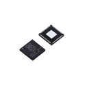
The RP2350, developed by Raspberry Pi Ltd, represents a significant advancement in the field of microcontrollers, building upon the foundation laid by its predecessor, the RP2040. This component is designed to cater to a wide range of applications requiring dual-core processing capabilities, with the option to switch between Dual Cortex-M33 or Hazard3 processors operating at up to 150 MHz. It features an extensive 520 kB of on-chip SRAM distributed across 10 independent banks, alongside 8 KB of one-time-programmable (OTP) storage. External memory interfaces are well-supported, with provisions for up to 16 MB of external QSPI flash/PSRAM, and an additional 16 MB accessible via an optional second chip-select, facilitating extensive code and data storage options. Security features are robust, including options for boot signing enforced by on-chip mask ROM, with key fingerprints stored in OTP, and hardware mitigations against fault injection attacks. The RP2350 also boasts a comprehensive set of peripherals, including 2x UARTs, 2x SPI controllers, 2x I2C controllers, 24x PWM channels, and a USB 1.1 controller with PHY for host and device support, among others. Programmable IO (PIO) state machines enhance its flexibility, enabling the implementation of custom peripherals. For developers, the RP2350 offers low-power operation modes and a built-in boot ROM that supports direct boot from external flash or OTP, serial boot from USB or UART, and secure boot with code signature enforcement. The device is available in QFN-60 (7x7 mm) and QFN-80 (10x10 mm) packages, with or without built-in flash, catering to diverse application requirements. This microcontroller is a compelling choice for sophisticated projects that demand high performance, extensive memory and peripheral support, and advanced security features.
62 Uses2 StarsMGM210LA22JIF
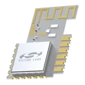
MGM210LA22JIF devices are PCB modules for Zigbee, Thread, Bluetooth and multiprotocol (Zigbee + Bluetooth) connectivity built around the EFR32MG21 Wireless Gecko Series 2 SoC and designed and optimized for the unique needs of smart LED lightbulbs. Delivering unparalleled RF performance and energy consumption compliance with CA Title 20, the module also offers a powerful and energy-efficient MCU core, 1024 kB of flash memory to enable future-proofing capabilities and over-the-air firmware updates with a dedicated core for enhanced security features. With its extended temperature rating and form factor, the device is suitable for enclosed operation in lightbulb housings. #CommonpartLibrary #Module #EFR32MG21 #arduino-matter
36 Uses2 StarsTinyFPGA-A-Schematic
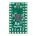
The schematic for TinyFPGA A-Series boards are tiny bare-bones FPGA boards created by Luke Valenty https://github.com/tinyfpga - Tiny, just 1.2 by 0.7 inches - Low power 3.3 volt operation - 18 user IOs (21 with JTAGEN) - 1200 4-input look-up tables - 10 kilobits distributed RAM - 64 kilobits dedicated RAM - 64 kilobits user flash memory - 1 SPI Hard-IP - 2 I2C Hard-IPs - 1 PLL Hard-IP - Built-in flash configuration memory programmable via JTAG
1 Uses2 StarsGL823K-HCY04
USB 2.0 single-LUN card reader controller supporting SD/MMC and Memory Stick PRO media, including SDHC/SDXC and microSD applications. Provides USB 2.0 High-Speed data transfer up to 480 Mbps and integrates an 8051 MCU, USB transceiver, FIFO, POR/LVD, card-power MOSFETs, and 5 V-to-3.3 V / 3.3 V-to-1.8 V regulators. Operates from 4.75 V to 5.25 V with typical active current of 50 mA and idle current of 45 mA; 0 °C to +70 °C operating temperature. Includes an on-chip clock source, eliminating the need for an external 12 MHz crystal. Available in SSOP-16 (150 mil). #USB2 #CardReader #SD #MMC #MemoryStick #InterfaceController #GENESYS
13 Uses1 StarsSTM32MP257FAI3
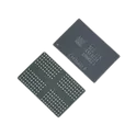
MPU with Dual Arm Cortex-A35 @1.5GHz, Cortex-M33 @400MHz, 3xEthernet (2+1 switch), 3xFD-CAN, LVDS/DSI, H.264, 3D GPU, AI/NN, Secure Boot, Cryptography, DRAM enc/dec, PKA The STM32MP257FAI3 is a high-performance microprocessor from STMicroelectronics' STM32MP2 series, integrating dual 64-bit Arm Cortex-A35 cores running at up to 1.5 GHz, a Cortex-M33 real-time core, and a Cortex-M0+ low-power management core. It is designed for advanced industrial, edge AI, machine vision, HMI, IoT gateway, and multimedia applications requiring Linux-class processing alongside deterministic real-time control. The device features AI acceleration, 3D graphics, video encoding/decoding, extensive connectivity, advanced security, and support for high-speed external memory. Key Features Dual-core 64-bit Arm Cortex-A35 CPU operating up to 1.5 GHz Arm Cortex-M33 real-time processor with TrustZone and FPU support Arm Cortex-M0+ low-power coprocessor for autonomous operation Integrated NPU (Neural Processing Unit) delivering up to 1.35 TOPS AI performance 3D GPU and hardware video encoder/decoder acceleration Supports DDR3L, DDR4, and LPDDR4 external memory up to 4 GB Multiple display interfaces including MIPI-DSI, LVDS, and parallel RGB USB 2.0 Host and USB 3.0 Dual-Role with embedded PHYs PCI Express interface with integrated 5 Gbps PHY Up to three Gigabit Ethernet interfaces with TSN and IEEE 1588 support Extensive connectivity: I2C, I3C, SPI, UART, USART, CAN FD, SDMMC, SAI, and SPDIF Hardware cryptographic accelerators including AES, SHA, RSA, ECC, PKA, and True RNG Secure boot, TrustZone security, tamper detection, and resource isolation framework Multiple low-power operating modes for energy-efficient designs Available in fine-pitch BGA packages for high-density embedded systems. #STM32MP257FAI3 #STM32MP2 #STMicroelectronics #CortexA35 #CortexM33 #EdgeAI #EmbeddedLinux #IndustrialAutomation #MachineVision #HMI #IoTGateway #MPU #PCIe #USB3 #GigabitEthernet #TrustZone #EmbeddedSystems #ArtificialIntelligence #LinuxProcessor #IndustrialIoT #CommonPartsLibrary #IntegratedCircuit #Microprocessor #STM32MP2
35 Uses1 Stars