Interface ICs
S32K344EHT1VPBST
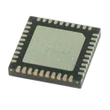
ARM® Cortex®-M7 S32K3 Microcontroller IC 32-Bit 160MHz 4MB (4M x 8) FLASH 172-QFP (16x16) S32K344EHT1VPBST is an automotive-grade 32-bit microcontroller from NXP Semiconductors based on the Arm Cortex-M7 core architecture. The device is designed for high-performance real-time automotive body, chassis, powertrain, and domain control applications requiring functional safety, security, and advanced communication interfaces. It integrates high-speed processing capability, extensive peripheral integration, hardware security acceleration, and deterministic control functions suitable for safety-critical embedded systems. The microcontroller operates with an Arm Cortex-M7 CPU core running at high frequency with floating-point support and DSP extensions for computationally intensive applications. Integrated flash memory and SRAM provide embedded program and data storage optimized for automotive embedded control systems. The device supports hardware-assisted security features including secure boot, cryptographic acceleration, and tamper protection for secure automotive network communication and firmware integrity. The S32K344EHT1VPBST includes multiple communication peripherals supporting CAN FD, FlexCAN, LIN, SPI, UART, I2C, and Ethernet interfaces for distributed automotive networking and gateway applications. Advanced analog integration includes ADC modules, timers, PWM generators, watchdogs, and motor-control-oriented peripherals enabling precision sensing and control functionality. The device supports functional safety development aligned with ISO 26262 requirements and includes error correction, memory protection, fault monitoring, and safety management features. Power management functionality supports low-power operating modes for energy-efficient automotive electronic control units. The microcontroller is housed in a thermally enhanced LQFP package suitable for automotive operating environments with extended temperature capability and AEC-Q100 qualification for automotive reliability standards. #commonpartslibrary #integratedcircuit #microcontroller #arm #m7
7 Uses
1 Star
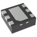
TMP117AIDRVR
Temperature Sensor Digital, Local -55°C ~ 150°C 16 b 6-WSON (2x2) The TMP117AIDRVR is a high-precision digital temperature sensor manufactured by Texas Instruments. The device provides accurate temperature measurements through an I²C-compatible digital interface and is optimized for applications requiring medical-grade accuracy, low power consumption, and compact PCB footprint. The sensor integrates a precision temperature sensing element, analog-to-digital converter, calibration memory, and digital interface into a single compact package. The device supports continuous conversion and shutdown operating modes, enabling efficient thermal monitoring in battery-powered and always-on systems. Internal calibration minimizes external component requirements while providing highly linear and repeatable temperature measurements across an extended operating range. The TMP117AIDRVR is commonly used in industrial controls, wearable electronics, healthcare equipment, environmental monitoring systems, battery management systems, consumer electronics, and precision instrumentation. Electrical Characteristics Supply voltage supports low-voltage digital systems and portable electronics applications. Ultra-low operating current enables long battery life in energy-sensitive designs. Integrated EEPROM allows programmable offset correction and configuration storage. Digital output eliminates the need for external ADC circuitry. High measurement resolution supports precision thermal monitoring applications. Low self-heating characteristics improve measurement stability and accuracy. Functional Features High-accuracy digital temperature sensing. I²C and SMBus compatible communication interface. Programmable alert functionality for thermal threshold monitoring. Continuous conversion and low-power shutdown operating modes. Integrated non-volatile memory for user configuration storage. Wide operating temperature range for industrial and commercial environments. Fast conversion timing suitable for real-time monitoring systems. Factory-calibrated performance requiring minimal external calibration. Package Information Package type is WSON with compact surface-mount footprint suitable for dense PCB layouts. Moisture-sensitive package designed for automated assembly processes. Lead-free and RoHS-compliant construction. Typical Applications Medical thermometers and patient monitoring systems. Industrial temperature monitoring equipment. Battery-powered portable electronics. HVAC and environmental sensing systems. Data acquisition and instrumentation systems. Server and embedded thermal management applications. Consumer electronics requiring precision thermal sensing. #commonpartslibrary #integratedcircuit #temperaturesensor
290 Uses
1 Star
PCA9685PW,118
LED Driver IC 16 Output Linear PWM Dimming 25mA 5.5V 28-TSSOP PCA9685PW,118 is a 16-channel, 12-bit PWM LED controller with an I²C interface designed for LED dimming, RGB/RGBA lighting, and servo motor control applications. It provides independent PWM control for up to 16 outputs, allowing precise brightness or position control while minimizing MCU GPIO usage. The device supports Fast-mode Plus I²C communication up to 1 MHz and operates from a 2.3 V to 5.5 V supply range. It is commonly used in robotics, LED backlighting, automation systems, and PWM expansion modules for microcontrollers such as Arduino, ESP32, and Raspberry Pi. Key Features 16 independent PWM output channels 12-bit PWM resolution (4096 steps) Programmable PWM frequency from approximately 24 Hz to 1526 Hz I²C Fast-mode Plus compatible interface up to 1 MHz Six hardware address pins allowing up to 62 devices on one I²C bus Programmable open-drain or totem-pole outputs Output capability: 25 mA sink current 10 mA source current Internal 25 MHz oscillator with optional external clock input Individual programmable LED ON/OFF timing for reduced EMI and current surges Supports software reset and group addressing (All Call/Sub Call) 5.5 V tolerant inputs and outputs Operating voltage range: 2.3 V to 5.5 V Package: 28-pin TSSOP (PW suffix) #CommonPartsLibrary #IntegratedCircuit #PowerManagement #LEDdriver
72 Uses
1 Star
STM32F405RGT6
ARM® Cortex®-M4 series Microcontroller IC 32-Bit Single-Core 168MHz 1MB (1M x 8) FLASH 64-LQFP (10x10) Arm® Cortex®-M4 32b MCU+FPU, 210DMIPS, up to 1MB flash/192+4KB RAM, USB OTG HS/FS, Ethernet, 17 TIMs, 3 ADCs, 15 comm. interfaces, and camera Includes ST state-of-the-art patented technology • Core: Arm® 32-bit Cortex®-M4 CPU with FPU, Adaptive real-time accelerator (ART Accelerator) allowing 0-wait state execution from flash memory, frequency up to 168 MHz, memory protection unit, 210 DMIPS/ 1.25 DMIPS/MHz (Dhrystone 2.1), and DSP instructions • Memories – Up to 1 Mbyte of flash memory – Up to 192+4 Kbytes of SRAM including 64- Kbyte of CCM (core coupled memory) data RAM – 512 bytes of OTP memory – Flexible static memory controller supporting CompactFlash™, SRAM, PSRAM, NOR and NAND memories • LCD parallel interface, 8080/6800 modes • Clock, reset, and supply management – 1.8 V to 3.6 V application supply and I/Os – POR, PDR, PVD and BOR – 4-to-26 MHz crystal oscillator – Internal 16 MHz factory-trimmed RC (1% accuracy) – 32 kHz oscillator for RTC with calibration – Internal 32 kHz RC with calibration • Low-power operation – Sleep, Stop, and Standby modes –VBAT supply for RTC, 20×32-bit backup registers + optional 4 KB backup SRAM • 3×12-bit, 2.4 MSPS A/D converters: up to 24 channels and 7.2 MSPS in triple interleaved mode • 2×12-bit D/A converters • General-purpose DMA: 16-stream DMA controller with FIFOs and burst support • Up to 17 timers: up to twelve 16-bit and two 32- bit timers up to 168 MHz, each with up to 4 IC/OC/PWM or pulse counter and quadrature (incremental) encoder input • Debug mode – Serial wire debug (SWD) & JTAG interfaces – Cortex-M4 Embedded Trace Macrocell™ • Up to 140 I/O ports with interrupt capability – Up to 136 fast I/Os up to 84 MHz – Up to 138 5 V-tolerant I/Os • Up to 15 communication interfaces – Up to 3 × I2C interfaces (SMBus/PMBus) – Up to 4 USARTs/2 UARTs (10.5 Mbit/s, ISO 7816 interface, LIN, IrDA, modem control) – Up to 3 SPIs (42 Mbits/s), 2 with muxed full-duplex I2S to achieve audio class accuracy via internal audio PLL or external clock – 2 × CAN interfaces (2.0B Active) – SDIO interface • Advanced connectivity – USB 2.0 full-speed device/host/OTG controller with on-chip PHY – USB 2.0 high-speed/full-speed device/host/OTG controller with dedicated DMA, on-chip full-speed PHY and ULPI – 10/100 Ethernet MAC with dedicated DMA: supports IEEE 1588v2 hardware, MII/RMII #commonpartslibrary #integratedcircuit #microcontroller
56 Uses
1 Star
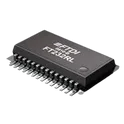
FT232RL
USB to Serial Interface, SSOP-28 FTDI USB Serial SSOP*5.3x10.2mm*P0.65mm* The FT232RL is a full-speed USB 2.0 to asynchronous serial data transfer IC. It integrates all the necessary USB protocol handling and UART interface logic, making it very easy to add USB connectivity to embedded devices without requiring complex firmware development. It is commonly used in development boards (like Arduino clones), USB-to-TTL converters, and debugging interfaces. Key Features USB Interface Fully compliant with USB 2.0 Full-Speed (12 Mbps) Integrated USB transceiver (no external components required) Supports USB suspend/resume modes Internal EEPROM for storing USB descriptors (no external EEPROM needed) Serial (UART) Interface Supports standard UART communication (TX, RX) Configurable baud rates from 300 bps up to 3 Mbps Supports hardware flow control (RTS/CTS, DTR/DSR) Bit-bang mode for simple GPIO control Integrated Components Built-in clock generator (no external crystal required) Internal EEPROM for configuration Integrated voltage regulator (3.3V output available for external use) Power Features Operates from 3.3V to 5V Can be powered directly from USB (bus-powered) Low power consumption with sleep mode Driver Support Virtual COM Port (VCP) drivers available for: Windows Linux macOS Also supports direct D2XX driver for advanced applications Package Typically available in SSOP-28 package Common Applications USB-to-serial converters (TTL/RS232) Microcontroller programming and debugging Embedded system communication Industrial and instrumentation interfaces
152 Uses
1 Star
ADXL335BCPZ
Accelerometer X, Y, Z Axis ±3g 1.6kHz (X,Y), 550Hz (Z) 16-LFCSP-LQ (4x4) The ADXL335BCPZ is a small, thin, low-power, complete 3-axis accelerometer with signal-conditioned voltage outputs. It measures acceleration with a minimum full-scale range of ±3 g. The device outputs analog voltages proportional to acceleration in each of the three orthogonal axes (X, Y, and Z). The accelerometer is designed for low power consumption and high resolution, making it suitable for mobile devices, tilt sensing, motion detection, and vibration monitoring. It operates over a wide temperature range and requires minimal external components, enabling easy integration into compact systems. Functional Overview The ADXL335 uses a capacitive sensing structure to detect acceleration. Changes in acceleration result in differential capacitance changes, which are converted into voltage outputs through an internal signal conditioning circuit. Each axis provides an independent analog output that can be directly interfaced with ADC inputs of microcontrollers or other processing units. Bandwidth for each axis can be adjusted using external capacitors, allowing flexibility depending on application requirements. Electrical Characteristics Supply Voltage Range: 1.8 V to 3.6 V Supply Current: Typical: 350 µA Measurement Range: ±3 g Sensitivity (Typical): 300 mV/g Zero-g Bias Level: Approximately mid-supply voltage Bandwidth: User-selectable via external capacitors Typical range: X, Y axes: up to 1600 Hz Z axis: up to 550 Hz Output Characteristics Output Type: Analog voltage (ratiometric to supply voltage) Number of Axes: Three (X, Y, Z) Output Noise: Low noise suitable for precision motion sensing Cross-Axis Sensitivity: Typically ±1% Mechanical Characteristics Package Type: 16-lead LFCSP (Lead Frame Chip Scale Package) Dimensions: Approximately 4 mm × 4 mm × 1.45 mm Mounting: Surface mount Environmental Specifications Operating Temperature Range: −40°C to +85°C Shock Survivability: Up to 10,000 g Interface Requirements External Components: Requires capacitors for bandwidth setting (one per axis) Output Interface: Direct analog output compatible with ADC inputs Applications Mobile devices and handheld electronics Tilt and orientation sensing Vibration monitoring systems Gaming and motion input devices Industrial instrumentation Wearable electronics Key Features Low power consumption Compact form factor High resolution analog outputs User-adjustable bandwidth Wide operating temperature range Simple integration with minimal external components #commonpartslibrary #sensor #transducer #motionsensor #accelerometer
58 Uses
1 Star
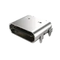
USB4105-GF-A
USB-C (USB TYPE-C) USB 2.0 Receptacle Connector 24 (16+8 Dummy) Position Surface Mount, Right Angle; Through Hole The USB4105-GF-A is a USB Type-C receptacle connector designed for USB 2.0 applications, commonly used in embedded systems, IoT devices, and consumer electronics. It features a 24-position (16 active + 8 dummy) contact design that supports reversible plug orientation, making it user-friendly and compliant with USB Type-C standards. This connector is a right-angle, surface-mount (SMT) device with through-hole retention tabs, providing both compact PCB integration and strong mechanical stability. Key Features USB Type-C Interface Reversible plug orientation (no wrong insertion) Standard USB Type-C receptacle Supports USB 2.0 signaling Contact Configuration 24 pins total (16 active + 8 dummy pins) Includes: Power (VBUS) Ground (GND) USB 2.0 data (D+, D−) Configuration channel (CC) Electrical Capability Supports multiple current levels (up to 5A depending on design) Rated voltage up to 48V DC Mechanical Design Right-angle (horizontal) mounting Surface-mount + through-hole hybrid Includes: Board guide Solder retention tabs (strong anchoring) Durability & Materials Shielded metal shell (EMI protection) Contact finish: Gold plating Housing: UL94 V-0 flame rated Mating cycles: ~20,000 insertions Environmental Specs Operating temperature: -40°C to +85°C RoHS compliant (lead-free) Typical Applications Microcontroller boards (ESP32, Arduino, etc.) Charging + data interface for embedded devices Power + USB communication ports Consumer electronics (gadgets, accessories) #CommonPartsLibrary #Connector #USB #DVI #USB4105 #USB-C
1.9k Uses
1 Star
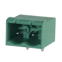
Phoenix Contact 1757242
2 Position Terminal Block Header, Male Pins, Shrouded (4 Side) 0.200" (5.08mm) 90°, Right Angle Through Hole Phoenix Contact MSTBA 2.5/ 2-G-5.08 CAN connector terminal block 2 pin The component is a two-position pluggable terminal block header designed for secure and reliable wire-to-board connections in industrial and embedded electronic systems. It is part of the COMBICON MSTB family, widely used for field wiring applications such as CAN bus, RS485, and power distribution. The device provides a robust interface between PCB circuitry and external wiring, supporting easy installation, maintenance, and replacement through a pluggable connection system. Mechanical Characteristics Number of Positions: 2 Pitch: 5.08 mm Mounting Type: Through-hole PCB mount Orientation: Vertical (straight) Termination Style: Pin header for mating plug connector Housing Material: Polyamide (PA), high-temperature resistant Color: Green Electrical Characteristics Rated Voltage: Up to 250 V Rated Current: Up to 12 A Contact Material: Copper alloy Contact Plating: Tin plated Environmental Characteristics Operating Temperature Range: -40°C to +105°C Flammability Rating: UL94 V-0 Mating and Compatibility Compatible Plug Series: Phoenix Contact MSTB 2,5 series (e.g., 1757019) Connection Method (Plug Side): Screw clamp termination Wire Size Range: Typically accepts 24 AWG to 12 AWG (depending on mating plug) Standards and Compliance RoHS: Compliant UL Recognized: Yes IEC Compliance: Yes Application Notes The component is commonly used in industrial communication systems such as CAN bus networks where a reliable and removable connection is required for CANH and CANL signals. Its 5.08 mm pitch ensures adequate spacing for signal integrity and ease of wiring, while the pluggable design simplifies field servicing and module replacement. #connector #tht #terminalblock
1.5k Uses
1 Star
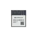
ESP32-C3-WROOM-02-N4
Bluetooth, WiFi 802.11b/g/n, Bluetooth v5.0 Transceiver Module 2.4GHz PCB Trace Surface Mount The ESP32-C3-WROOM-02-N4 is a compact, general-purpose Wi-Fi and Bluetooth Low Energy (BLE) module developed by Espressif Systems. It is built around the ESP32-C3 SoC and integrates RF components, crystal oscillator, flash memory, and PCB antenna in a single module. It is designed for a wide range of applications such as IoT devices, smart home systems, industrial automation, and consumer electronics, offering a balance of performance, low power consumption, and cost efficiency. Key Features MCU & Memory 32-bit RISC-V single-core processor up to 160 MHz 384 KB ROM 400 KB SRAM + 8 KB RTC SRAM Integrated 4 MB SPI flash (N4 variant) Connectivity 2.4 GHz Wi-Fi (802.11 b/g/n) Supports Station, SoftAP, and Station + SoftAP modes Bluetooth 5 (BLE) with mesh support Data rates up to 150 Mbps (Wi-Fi) Peripherals & Interfaces Up to 15 GPIOs Interfaces: SPI, UART, I2C, I2S LED PWM ADC (SAR) Timers & watchdog USB Serial/JTAG support TWAI® (CAN 2.0 compatible) #commonpartslibrary #transceiver #module #wireless #rf
946 Uses
1 Star
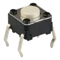
B3F-1000
Tactile Switch SPST-NO Top Actuated Through Hole tactile switch 6x6 through hole The B3F-1000 is a compact, through-hole mounted tactile switch designed for momentary input applications. It features a standard 6.0 mm square footprint and is widely used in consumer and industrial electronics for reliable user interface control. Mechanical Characteristics Dimensions (L × W × H): 6.0 mm × 6.0 mm × 3.4 mm Actuator Type: Round Actuator Height: 4.3 mm Mounting Style: Through Hole Mounting Direction: Straight Termination Style: Solder Pin Color: White Electrical Characteristics Switch Function: SPST, Momentary (OFF-(ON)) Contact Rating: 50 mA @ 24 VDC Operating Force: 1 N (~100 gf) Contact Resistance: ≤100 mΩ (typical, refer to datasheet) Insulation Resistance: ≥100 MΩ (typical, refer to datasheet) Environmental Characteristics Operating Temperature Range: -25°C to +70°C RoHS Compliance: Yes Reliability Operating Life: 1,000,000 cycles Packaging Information Factory Pack Quantity: 1500 pcs Unit Weight: 0.008818 oz (~0.25 g) Additional Information Country of Origin: Japan (JP) Illumination: Non-illuminated Ground Terminal: No #commonpartslibrary #switch #tactile #spst
1.6k Uses
1 Star

CH32X035F7P6
The CH32X035/X033 series, developed by WCH, encompasses industrial-grade microcontrollers based on the QingKe RISC-V core. These microcontrollers, including models such as the CH32X035R8T6, CH32X035C8T6, CH32X035G8U6, CH32X035G8R6, CH32X035F8U6, CH32X035F7P6, and CH32X033F8P6, are equipped with integrated USB and PD PHY, supporting USB Host and Device functionalities, as well as PDUSB and Type-C fast charging capabilities. The series features a programmable protocol I/O controller, two groups of operational amplifiers (OPA), three groups of comparators (CMP), four USARTs, I2C, SPI, multiple timers, a 12-bit ADC, and 14-channel capacitive touch-key interfaces, among other peripherals. These microcontrollers offer a comprehensive suite of features, including a 32-bit QingKe RISC-V4C core with support for the RV32IMAC instruction set, fast interrupt handling, and low-power modes, making them suitable for a wide range of embedded applications. With a robust memory architecture comprising 20KB SRAM and 62KB CodeFlash, alongside various power management and security features, the CH32X035/X033 series is designed to deliver high performance and flexibility for industrial applications.
5 Uses
1 Star
ICM-20948
The TDK InvenSense ICM-20948 is the world's lowest power 9-axis MotionTracking™ device, optimized for Smartphones, Tablets, Wearable Sensors, and IoT applications. This highly integrated component features a 3-axis gyroscope, 3-axis accelerometer, and 3-axis compass, all housed within a compact 3 mm x 3 mm x 1 mm 24-pin QFN package. The ICM-20948 includes an onboard Digital Motion Processor™ (DMP™) that offloads motion processing algorithms from the host processor, thereby enhancing overall system power performance. It supports both I2C and high-speed SPI communication interfaces and operates within a voltage range of 1.71V to 3.6V. The device is fully compliant with Google's latest Android release and supports EIS FSYNC. Additional features include on-chip 16-bit ADCs, programmable digital filters, an embedded temperature sensor, and programmable interrupts, making it an ideal choice for applications requiring precise motion tracking and low power consumption.
114 Uses
1 Star
PS21964-4S
The Mitsubishi PS21964-4S is a dual-in-line package intelligent power module that integrates a transfer-mold type insulated design suitable for 600V/15A applications. This component combines low-loss 5th generation IGBT inverter bridge technology dedicated to three-phase DC-to-AC power conversion with open emitter configuration. It is designed with embedded drive circuits, high voltage high-speed level shifting, under-voltage protection for both upper and lower leg IGBTs, short circuit protection for lower-leg IGBTs, and system control functionalities into a compact package. The module supports fault signaling corresponding to short circuit faults in the lower-leg IGBT or under-voltage conditions, offering an integrated solution for AC100V~200V inverter drive applications in small power motor controls. With its UL approval (Yellow Card No. E80276) and featuring an input interface compatible with 3V and 5V lines (High Active), the PS21964-4S is engineered to cater to a broad range of industrial applications demanding reliable and efficient power conversion and control.
28 Uses
1 Star