Transistors
A transistor is a type of electronic device that controls the flow of electricity or current through a circuit. It acts as a switch or gate, allowing current to pass through or blocking it, depending on the input signal applied to the transistor. Transistors are widely used in a variety of electronic devices and systems, including computers, televisions, radios, and smartphones. They are also used in a range of industrial and medical applications, such as power supply systems and medical equipment. Flux.ai is home to the world's largest community-driven public library of transistors, with footprints, symbols, datasheets, and simulation models available for a wide range of devices. The library is constantly being updated and expanded by a community of engineers and enthusiasts, making it an invaluable resource for anyone working with transistors. Whether you're a student, hobbyist, or professional engineer, you'll find everything you need to know about transistors at Flux.ai.
IRLR7843TRPBF
N-Channel 30 V 161A (Tc) 140W (Tc) Surface Mount TO-252AA (DPAK) The IRLR7843TRPBF is an N-channel power MOSFET built on Infineon's HEXFET technology platform, originally developed by International Rectifier. It is designed as a low-voltage, high-current switching device intended for applications where minimizing conduction loss and maximizing efficiency are primary design goals. The part is particularly well suited to synchronous switching topologies, where pairs or arrays of MOSFETs alternately conduct to regulate power flow with minimal energy dissipation. This device targets high-density power conversion applications where board space is limited but current demands are substantial, such as notebook computer power delivery, point-of-load converters used in servers, and advanced telecom and datacom equipment. It is commonly found supporting synchronous buck converter stages that step down a higher input rail to a lower output voltage suitable for powering processors, memory, and other low-voltage digital logic. Its low on-resistance characteristic allows it to carry significant current while generating comparatively little resistive heating, which is essential in compact enclosures with constrained thermal budgets. The transistor is fabricated using a refined trench gate process that improves upon earlier HEXFET generations, offering reduced gate charge and lower switching losses alongside its low conduction resistance. This combination makes it effective in both the high-side and low-side positions of a synchronous switching cell, where fast, clean transitions reduce overlap losses and improve overall converter efficiency. The device also offers well-characterized avalanche energy ratings, giving designers confidence in its ruggedness when exposed to transient overvoltage events that can occur during switching, and it presents a very low gate impedance, allowing it to be driven efficiently by standard gate driver circuitry. Mechanically, the part is housed in a surface-mount power package with an exposed tab for enhanced thermal conduction to the host PCB, allowing heat generated during operation to be efficiently transferred away from the silicon die. This package style is widely used in power-dense designs where through-hole packages would be impractical. The device is supplied in a tape-and-reel format suitable for automated assembly and is compliant with RoHS material restrictions, reflecting current environmental and regulatory standards for electronic components. Spec Sheet Identification Part Number: IRLR7843TRPBF Device Family: HEXFET Power MOSFET Manufacturer: Infineon Technologies Functional Classification Device Type: Power MOSFET Channel Type: N-channel Technology: Trench-gate HEXFET (IR MOSFET legacy technology) Logic Level Compatibility: Logic-level gate drive compatible Electrical Characteristics Drain-to-Source Voltage Rating: Low-voltage class, optimized for sub-30V rail applications On-Resistance: Ultra-low on-resistance class Drain Current Capability: High continuous current class Gate Charge: Low gate charge, optimized for fast switching Gate Impedance: Ultra-low gate impedance Avalanche Characteristics: Fully characterized avalanche voltage and current rating Switching & Application Behavior Primary Application: Synchronous buck converter switching stages Suitable Position: High-side and low-side switch positions Target Use Cases: Point-of-load conversion, notebook power delivery, telecom/datacom power systems Thermal & Mechanical Package Type: Surface-mount power package with exposed thermal tab (DPAK-style) Mounting: Surface mount technology (SMT) Thermal Path: Tab-based conduction to PCB for heat dissipation Environmental & Qualification RoHS Compliance: Yes Lifecycle Status: Active production Packaging Format Supply Format: Tape-and-reel, per part suffix designation #IRLR7843 #Infineon #HEXFET #PowerMOSFET #NChannelMOSFET #SynchronousBuck #PowerElectronics #DCDCConverter #PointOfLoad #PowerConversion #DPAK #SMTPackage #RoHSCompliant #SemiconductorIC #EngineeringSpec #ComponentLibrary #CommonPartsLibrary #PowerDensity #LowRDSon #DiscreteSemiconductor #commonpartslibrary #transistor
3 Uses0 StarsIXFH120N15P
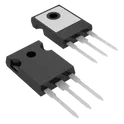
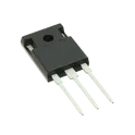
N-Channel 200 V 120A (Tc) 714W (Tc) Through Hole TO-247AD (IXFH) # IXFH120N15P ## General Description The IXFH120N15P is a high-current N-channel power MOSFET manufactured by Littelfuse IXYS. It is designed for demanding power switching and power conversion applications requiring low conduction losses, fast switching performance, and high current-handling capability. Built using advanced power MOSFET technology, the device provides excellent efficiency, ruggedness, and thermal performance for industrial power systems, motor drives, battery management equipment, welding systems, uninterruptible power supplies, renewable energy systems, and high-power DC switching applications. Its robust construction and low on-state resistance make it particularly suitable for designs requiring high efficiency and reliable operation under heavy load conditions. ## Key Features ### Power MOSFET Architecture * N-channel enhancement-mode MOSFET * Advanced power semiconductor technology * Low conduction losses * High-current switching capability * Optimized efficiency for power conversion applications * Fast switching performance ### Electrical Characteristics * Low on-state resistance * High-current carrying capability * Low gate drive power requirements * Excellent switching efficiency * Stable electrical performance under demanding operating conditions * Suitable for high-power applications ### Switching Performance * Fast turn-on characteristics * Fast turn-off characteristics * Reduced switching losses * High-frequency operation capability * Efficient power control functionality ### Thermal Characteristics * High power dissipation capability * Excellent thermal conductivity * Efficient heat transfer performance * Suitable for heatsink mounting * Reliable operation under continuous load conditions ### Protection and Reliability * Avalanche ruggedness * Robust semiconductor structure * Enhanced reliability under transient conditions * Long operational service life * Industrial-grade durability ### Package Characteristics * Through-hole power package * Electrically isolated mounting configuration * Suitable for high-power assemblies * Automated and manual assembly compatibility * Industrial-grade mechanical construction ### Material Construction * Advanced silicon power MOSFET technology * High-reliability semiconductor materials * RoHS-compliant construction * Lead-free compatible package * Rugged power device architecture ### Environmental Characteristics * Suitable for industrial operating environments * High mechanical durability * Stable operation across extended temperature ranges * Reliable continuous-duty performance ### Application Areas * Motor Drive Systems * Industrial Power Supplies * Battery Management Systems * Renewable Energy Equipment * Solar Power Converters * DC-DC Converters * High-Power Switching Circuits * Welding Equipment * Uninterruptible Power Supplies * Electric Vehicle Support Systems * Energy Storage Systems * Industrial Automation Equipment ### Compliance * RoHS Compliant * Lead-Free Compatible * Industrial-Grade Power Semiconductor Solution ## Manufacturer Littelfuse IXYS ## Product Family PolarP N-Channel Power MOSFET Series #IXFH120N15P #IXYS #Littelfuse #PowerMOSFET #NChannelMOSFET #PowerElectronics #MotorDrive #DCDCConverter #PowerSupplyDesign #IndustrialElectronics #EnergyStorage #RenewableEnergy #BatteryManagement #ElectronicsEngineering #PowerSemiconductor #Commonpartslibrary #Transistor #MOSFET #FET #tht
0 Uses0 StarsNE555P
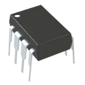
555 Type, Timer/Oscillator (Single) IC 100kHz 8-PDIP NE555 DIP-8 through hole The NE555P is a classic and widely used precision timer IC manufactured by companies like Texas Instruments and others. It belongs to the popular 555 timer family and is designed for generating accurate time delays, oscillations, and pulse signals. The “P” variant refers to the PDIP (Plastic Dual In-line Package), making it ideal for through-hole mounting, breadboarding, and prototyping. NE555P PDIP-8 timer Internally, the NE555P consists of: Two comparators A flip-flop A discharge transistor A voltage divider network These blocks allow flexible configuration for timing and waveform generation. Key Features Timing & Operation Modes Monostable mode (one-shot pulse generation) Astable mode (continuous oscillator) Bistable mode (flip-flop operation) Electrical Characteristics Supply voltage range: 4.5V to 16V Output can source or sink up to 200 mA Adjustable duty cycle Performance High timing accuracy and stability Timing range from microseconds to hours (depends on external R and C) Temperature-stable operation Package & Usability 8-pin DIP (through-hole) package Easy to use for: Breadboards DIY electronics Educational projects Common Applications LED flashers and blinkers Pulse generation Time delay circuits PWM control (e.g., dimming LEDs, motor speed control) Tone/sound generation #Timer #commonpartslibrary
1.9k Uses0 StarsIRLML6244TRPBF
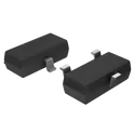
MOSFET N-CH 20V 6.3A SOT-23 The IRLML6244TRPBF is an N-channel enhancement-mode power MOSFET from Infineon Technologies (originally International Rectifier HEXFET series). It is designed for low-voltage power switching applications such as load switching, DC-DC converters, and LED control. It comes in a compact SOT-23 (Micro3™) surface-mount package, making it suitable for space-constrained PCB designs while still handling relatively high current for its size. Key Features Drain-Source Voltage (VDS): 20 V Continuous Drain Current: up to ~6.3 A (at 25°C) Very low RDS(on): ~21 mΩ @ VGS = 4.5 V ~27 mΩ @ VGS = 2.5 V Low gate threshold voltage (~0.5–1.1 V typical range) (note: not a switching guarantee) Gate-to-source voltage rating: ±12 V Low power loss due to low on-resistance High efficiency switching for low-voltage systems Power dissipation: ~1.3 W (thermal limited in SOT-23 package) Fast switching performance (low gate charge ~8.9 nC) Operating temperature range: −55°C to +150°C RoHS compliant (lead-free, halogen-free) Typical Applications Low-side load switching (MCUs, GPIO control) LED strip / RGB LED drivers Battery-powered systems DC-DC converter switching Small motor or relay driving General-purpose power management in compact electronics Important Design Note Even though it has a low VGS(th), this MOSFET is not selected based on threshold voltage. What matters is the RDS(on) at your gate drive voltage (2.5 V / 3.3 V / 5 V) to ensure it fully turns on with minimal heating. #CommonPartsLibrary #Transistor #FET #IRLML6244 #MOSFET #NChannelMOSFET #PowerElectronics #SOT23 #Infineon #HEXFET #LEDDriver #LowSideSwitch #ElectronicsComponents
218 Uses0 StarsAO3401
MOSFET P-CH 30V 4.1A SOT-23 The AO3401 is a 30 V P-Channel Enhancement Mode MOSFET designed for high-efficiency power switching applications. It uses advanced trench MOSFET technology to achieve low on-resistance (RDS(on)), low gate charge, and fast switching performance. Packaged in a compact SOT-23 package, it is widely used in load switching, battery-powered devices, reverse-polarity protection circuits, and power management applications. Key Features P-Channel MOSFET Drain-Source Voltage (VDS): −30 V Continuous Drain Current (ID): up to −4 A (25°C) Low RDS(on): 50 mΩ max @ VGS = −10 V 60 mΩ max @ VGS = −4.5 V 85 mΩ max @ VGS = −2.5 V Low Gate Charge: 7 nC typical @ 4.5 V Gate-Source Voltage Rating: ±12 V Low Threshold Voltage: −0.5 V to −1.3 V Fast Switching Characteristics Compact SOT-23 Surface-Mount Package Operating Junction Temperature: up to 150°C Suitable for Low-Voltage Logic-Level Drive Applications Typical Applications Load switches Battery protection circuits Reverse-polarity protection Power-path management DC-DC converters Portable and battery-powered electronics PWM switching applications #CommonPartsLibrary #Transistor #FET #Mosfet
27 Uses0 Stars6N137-560E
The Broadcom® 6N137, HCPL-26xx/06xx/4661, HCNW137/26x1 are optically coupled gates that combine a GaAsP light emitting diode and an integrated high gain photo detector. An enable input allows the detector to be strobed. The output of the detector IC is an open collector Schottky-clamped transistor. The internal shield provides a guaranteed common mode transient immunity specification up to 15,000 V/µs at Vcm = 1000V. This unique design provides maximum AC and DC circuit isolation while achieving TTL compatibility. The optocoupler AC and DC operational parameters are guaranteed from – 40°C to +85°C allowing trouble-free system performance. 15 kV/µs minimum Common Mode Rejection (CMR) at VCM= 1 kV for HCNW2611, HCPL-2611, HCPL-4661, HCPL-0611, HCPL-0661 High speed: 10 MBd typical LSTTL/TTL compatible Low input current capability: 5 mA Guaranteed AC and DC performance over temperature: –40°C to +85°C Available in 8-Pin DIP, SOIC-8, widebody packages Strobable output (single channel products only) Safety approval – UL recognized – 3750 Vrms for 1 minute and 5000 Vrms for 1 minute per UL1577 CSA approved (5000 Vrms/1 Minute rating is for HCNW137/26X1 and Option 020 [6N137, HCPL-2601/11/30/31, HCPL-4661] products only) – IEC/EN/DIN EN 60747-5-5 approved with: VIORM = 567 Vpeak for 06xx Option 060 VIORM = 630 Vpeak for 6N137/26xx Option 060 VIORM =1414 Vpeak for HCNW137/26x1 MIL-PRF-38534 hermetic version available (HCPL56xx/66xx) #CommonPartsLibrary #Isolator #Optocoupler
71 Uses0 StarsSI2300
The SI2300 is a N-channel enhancement-mode MOSFET designed for efficient switching and power management applications. Fabricated using advanced trench MOS technology, it delivers low on-state resistance, fast switching performance, and high current handling capability within a compact surface-mount package. The device is widely used in load switching, battery-powered equipment, DC-DC converters, motor control circuits, power distribution systems, and general-purpose switching applications where efficiency and space optimization are critical. Features N-channel enhancement-mode MOSFET Low on-state resistance for reduced conduction losses Fast switching characteristics Low gate charge for efficient drive operation Compact surface-mount package High current carrying capability Low power dissipation design Optimized for battery-operated systems Suitable for high-speed switching applications RoHS-compliant and lead-free construction Applications Power management circuits Load switching systems Battery protection modules Portable electronic devices DC-DC converter circuits Motor drive applications Power distribution networks Embedded control systems Consumer electronics Industrial automation equipment Electrical Characteristics Low drain-to-source on-resistance High drain current capability Low gate threshold voltage Fast turn-on and turn-off response Low gate capacitance High switching efficiency Low leakage current characteristics Enhanced thermal performance Stable operation across specified temperature ranges Reliable avalanche and transient performance Mechanical Characteristics Surface-mount package construction Compact footprint for high-density PCB layouts Suitable for automated assembly processes Compatible with standard reflow soldering methods Tape-and-reel packaging availability Robust package integrity for production environments Environmental Characteristics Industrial-grade reliability Resistance to mechanical shock and vibration within specification limits Moisture-resistant package design Suitable for operation in demanding electronic environments Compliant with RoHS and environmental regulations Long operational lifetime under recommended operating conditions #commonpartslibrary #mosfet #nchannelmosfet #powermanagement #powerswitching #semiconductor #transistor #loadswitch #dcdcconverter #batteryprotection #embeddedsystems #industrialelectronics #consumerelectronics #smtcomponent #electronicsdesign
326 Uses0 Stars