Voltage Regulators
X5521FV-2x15-C85D30-1150
Female Headers X5521FV-2x15-C85D30-1150 HDR-TH_30P-P2.54-V-F-R2-C15-S2.54-3 LCSC Part Number: C2916939 JLCPCB Part Class: Extended Part Manufactured by XKB Connectivity(中国星坤) XKB X5521FV-2xXX-C85D30-1150 dual-row female socket header connector, 2.54mm pitch, through-hole vertical mounting, round pin receptacle type, PPS UL94V-0 black insulator, brass outer sleeve with beryllium copper clip contact, tin or gold plating, 3A current rating, 1000V RMS dielectric withstand voltage, 10mΩ max contact resistance, 500 mating cycles mechanical life, -40°C to +105°C operating temperature, suitable for 0.635mm to 0.889mm mating pins. Search Keywords: XKB X5521FV, X5521FV-2xXX-C85D30-1150, XKB female socket header, XKB round pin socket, 2.54mm female socket header, 2.54mm dual row female header, 2x10 female socket header, 20 pin female header, through hole female header, vertical socket connector, round pin receptacle connector, machined pin female header, PPS UL94V-0 socket connector, XKB 2.54mm connector Hashtags: #XKB #X5521FV #X5521FV2xXXC85D301150 #FemaleHeader #SocketHeader #RoundPinSocket #MachinedPinSocket #ReceptacleConnector #254mmConnector #254mmPitch #DualRowHeader #2x10Header #20PinHeader #ThroughHoleConnector #VerticalConnector #PPSInsulator #UL94V0 #BerylliumCopperContact #BrassContact #3AConnector
46 Uses
1 Star
OV2640 Camera Board
Sensor Evaluation Boards RoHS The OV2640 Camera Board integrates the OV2640 2MP CameraChip™ sensor with onboard circuitry to simplify interfacing with microcontrollers. It captures images up to UXGA resolution (1622 × 1200 / 1632 × 1232 depending on configuration) and supports both raw and compressed output formats. The sensor also includes an internal image signal processor (ISP), allowing direct JPEG compression without external processing. This makes it especially suitable for low-cost embedded systems where bandwidth and MCU resources are limited. ⭐ Key Features 📸 Image Performance 2 Megapixel CMOS sensor (OV2640) Max resolution: UXGA (up to ~1600 × 1200 class) Frame rates (typical): UXGA / SXGA: up to ~15–30 fps (depending on mode) SVGA: up to 30 fps CIF: up to 60 fps 🎨 Output Formats Supports multiple image data formats: JPEG (hardware compressed) YUV 422 / 420 RGB565 / RGB555 YCbCr 4:2:2 8-bit raw / compressed output modes ⚡ Electrical Characteristics Supply voltage: 3.3V I/O voltage range: 1.7V – 3.3V Low-power CMOS design optimized for embedded devices
210 Uses
1 Star
TMP117AIDRVR
Temperature Sensor Digital, Local -55°C ~ 150°C 16 b 6-WSON (2x2) The TMP117AIDRVR is a high-precision digital temperature sensor manufactured by Texas Instruments. The device provides accurate temperature measurements through an I²C-compatible digital interface and is optimized for applications requiring medical-grade accuracy, low power consumption, and compact PCB footprint. The sensor integrates a precision temperature sensing element, analog-to-digital converter, calibration memory, and digital interface into a single compact package. The device supports continuous conversion and shutdown operating modes, enabling efficient thermal monitoring in battery-powered and always-on systems. Internal calibration minimizes external component requirements while providing highly linear and repeatable temperature measurements across an extended operating range. The TMP117AIDRVR is commonly used in industrial controls, wearable electronics, healthcare equipment, environmental monitoring systems, battery management systems, consumer electronics, and precision instrumentation. Electrical Characteristics Supply voltage supports low-voltage digital systems and portable electronics applications. Ultra-low operating current enables long battery life in energy-sensitive designs. Integrated EEPROM allows programmable offset correction and configuration storage. Digital output eliminates the need for external ADC circuitry. High measurement resolution supports precision thermal monitoring applications. Low self-heating characteristics improve measurement stability and accuracy. Functional Features High-accuracy digital temperature sensing. I²C and SMBus compatible communication interface. Programmable alert functionality for thermal threshold monitoring. Continuous conversion and low-power shutdown operating modes. Integrated non-volatile memory for user configuration storage. Wide operating temperature range for industrial and commercial environments. Fast conversion timing suitable for real-time monitoring systems. Factory-calibrated performance requiring minimal external calibration. Package Information Package type is WSON with compact surface-mount footprint suitable for dense PCB layouts. Moisture-sensitive package designed for automated assembly processes. Lead-free and RoHS-compliant construction. Typical Applications Medical thermometers and patient monitoring systems. Industrial temperature monitoring equipment. Battery-powered portable electronics. HVAC and environmental sensing systems. Data acquisition and instrumentation systems. Server and embedded thermal management applications. Consumer electronics requiring precision thermal sensing. #commonpartslibrary #integratedcircuit #temperaturesensor
287 Uses
1 Star
TLV62569DBVR
Buck Switching Regulator IC Positive Adjustable 0.6V Output 2A SC-74A, SOT-753 The Texas Instruments TLV62569DBVR is a high-efficiency synchronous step-down (buck) DC-DC converter designed for compact and low-power applications. It converts a higher DC input voltage down to a lower, regulated output voltage with high efficiency and small external component size. It is commonly used in portable electronics, embedded systems, routers, set-top boxes, and battery-powered devices where efficient power conversion and small footprint are important. 🔧 Key Features Input voltage range: 2.5 V to 5.5 V Output current capability: up to 2 A Adjustable output voltage: 0.6 V to VIN (via external resistors) High efficiency: up to ~95% Switching frequency: ~1.5 MHz (allows small inductors/capacitors) Synchronous rectification: improves efficiency by reducing losses Power Save Mode (PSM): boosts efficiency at light load Low quiescent current: ~35 µA typical 100% duty cycle support: low dropout operation 🛡️ Protection & Safety Features Overcurrent protection (OCP) Thermal shutdown protection Internal soft-start (reduces inrush current at startup) Power Good (PG) indicator for system monitoring 📦 Package SOT-23-5 (DBVR) Very small footprint for space-constrained PCB designs ⚙️ Typical Applications Point-of-load (POL) power supplies Wireless routers and networking devices Set-top boxes Battery-powered and portable systems Embedded controllers and IoT devices
59 Uses
1 Star
PCA9685PW,118
LED Driver IC 16 Output Linear PWM Dimming 25mA 5.5V 28-TSSOP PCA9685PW,118 is a 16-channel, 12-bit PWM LED controller with an I²C interface designed for LED dimming, RGB/RGBA lighting, and servo motor control applications. It provides independent PWM control for up to 16 outputs, allowing precise brightness or position control while minimizing MCU GPIO usage. The device supports Fast-mode Plus I²C communication up to 1 MHz and operates from a 2.3 V to 5.5 V supply range. It is commonly used in robotics, LED backlighting, automation systems, and PWM expansion modules for microcontrollers such as Arduino, ESP32, and Raspberry Pi. Key Features 16 independent PWM output channels 12-bit PWM resolution (4096 steps) Programmable PWM frequency from approximately 24 Hz to 1526 Hz I²C Fast-mode Plus compatible interface up to 1 MHz Six hardware address pins allowing up to 62 devices on one I²C bus Programmable open-drain or totem-pole outputs Output capability: 25 mA sink current 10 mA source current Internal 25 MHz oscillator with optional external clock input Individual programmable LED ON/OFF timing for reduced EMI and current surges Supports software reset and group addressing (All Call/Sub Call) 5.5 V tolerant inputs and outputs Operating voltage range: 2.3 V to 5.5 V Package: 28-pin TSSOP (PW suffix) #CommonPartsLibrary #IntegratedCircuit #PowerManagement #LEDdriver
70 Uses
1 Star
TXS0108EPWR
Voltage Level Translator Bidirectional 1 Circuit 8 Channel 60Mbps 20-TSSOP This device is an 8-bit non-inverting level translator which uses two separate configurable power-supply rails. The A port tracks the VCCA pin supply voltage. The VCCA pin accepts any supply voltage between 1.4V and 3.6V. The B port tracks the VCCB pin supply voltage. The VCCB pin accepts any supply voltage between 1.65V and 5.5V. Two input supply pins allows for low Voltage bidirectional translation between any of the 1.5V, 1.8V, 2.5V, 3.3V, and 5V voltage nodes. When the output-enable (OE) input is low, all outputs are placed in the high-impedance (Hi-Z) state. To put the device in the Hi-Z state during power-up or power-down periods, tie OE to GND through a pulldown resistor. The current-sourcing capability of the driver determines the minimum value of the resistor. • No direction-control signal needed • Maximum data rates: – 110Mbps (push pull) – 1.2Mbps (open drain) • 1.4V to 3.6V on A port and 1.65V to 5.5V on B port (VCCA ≤ VCCB) • No power-supply sequencing required – either VCCA or VCCB can be ramped first • Latch-up performance exceeds 100mA per JESD 78, class II • ESD protection exceeds JESD 22 (A port): – 2000 V Human Body Model (A114-B) – 150 V Machine Model (A115-A) – 1000 V Charged-Device Model (C101) • IEC 61000-4-2 ESD (B-port): – ± 8kV Contact Discharge – ± 6kV Air Discharge #commonpartslibrary #integratedcircuit #logic #translator #levelshifter
334 Uses
1 Star
HX711
Precision 24-bit analog-to-digital converter (ADC) designed for weigh scales and industrial control applications to interface directly with a bridge sensor. Based on Avia Semiconductor’s patented technology, HX711 is a precision 24-bit analogto-digital converter (ADC) designed for weigh scales and industrial control applications to interface directly with a bridge sensor. The input multiplexer selects either Channel A or B differential input to the low-noise programmable gain amplifier (PGA). Channel A can be programmed with a gain of 128 or 64, corresponding to a full-scale differential input voltage of ±20mV or ±40mV respectively, when a 5V supply is connected to AVDD analog power supply pin. Channel B has a fixed gain of 32. Onchip power supply regulator eliminates the need for an external supply regulator to provide analog power for the ADC and the sensor. Clock input is flexible. It can be from an external clock source, a crystal, or the on-chip oscillator that does not require any external component. On-chip poweron-reset circuitry simplifies digital interface initialization. There is no programming needed for the internal registers. All controls to the HX711 are through the pins. • Two selectable differential input channels • On-chip active low noise PGA with selectable gain of 32, 64 and 128 • On-chip power supply regulator for load-cell and ADC analog power supply • On-chip oscillator requiring no external component with optional external crystal • On-chip power-on-reset • Simple digital control and serial interface: pin-driven controls, no programming needed • Selectable 10SPS or 80SPS output data rate • Simultaneous 50 and 60Hz supply rejection • Current consumption including on-chip analog power supply regulator: normal operation < 1.5mA, power down < 1uA • Operation supply voltage range: 2.6 ~ 5.5V • Operation temperature range: -40 ~ +85℃ • 16 pin SOP-16 package #commonpartslibrary #integratedcircuit #analog #digital #converter #sensor
797 Uses
1 Star
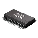
FT232RL
USB to Serial Interface, SSOP-28 FTDI USB Serial SSOP*5.3x10.2mm*P0.65mm* The FT232RL is a full-speed USB 2.0 to asynchronous serial data transfer IC. It integrates all the necessary USB protocol handling and UART interface logic, making it very easy to add USB connectivity to embedded devices without requiring complex firmware development. It is commonly used in development boards (like Arduino clones), USB-to-TTL converters, and debugging interfaces. Key Features USB Interface Fully compliant with USB 2.0 Full-Speed (12 Mbps) Integrated USB transceiver (no external components required) Supports USB suspend/resume modes Internal EEPROM for storing USB descriptors (no external EEPROM needed) Serial (UART) Interface Supports standard UART communication (TX, RX) Configurable baud rates from 300 bps up to 3 Mbps Supports hardware flow control (RTS/CTS, DTR/DSR) Bit-bang mode for simple GPIO control Integrated Components Built-in clock generator (no external crystal required) Internal EEPROM for configuration Integrated voltage regulator (3.3V output available for external use) Power Features Operates from 3.3V to 5V Can be powered directly from USB (bus-powered) Low power consumption with sleep mode Driver Support Virtual COM Port (VCP) drivers available for: Windows Linux macOS Also supports direct D2XX driver for advanced applications Package Typically available in SSOP-28 package Common Applications USB-to-serial converters (TTL/RS232) Microcontroller programming and debugging Embedded system communication Industrial and instrumentation interfaces
150 Uses
1 Star
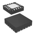
ADXL335BCPZ
Accelerometer X, Y, Z Axis ±3g 1.6kHz (X,Y), 550Hz (Z) 16-LFCSP-LQ (4x4) The ADXL335BCPZ is a small, thin, low-power, complete 3-axis accelerometer with signal-conditioned voltage outputs. It measures acceleration with a minimum full-scale range of ±3 g. The device outputs analog voltages proportional to acceleration in each of the three orthogonal axes (X, Y, and Z). The accelerometer is designed for low power consumption and high resolution, making it suitable for mobile devices, tilt sensing, motion detection, and vibration monitoring. It operates over a wide temperature range and requires minimal external components, enabling easy integration into compact systems. Functional Overview The ADXL335 uses a capacitive sensing structure to detect acceleration. Changes in acceleration result in differential capacitance changes, which are converted into voltage outputs through an internal signal conditioning circuit. Each axis provides an independent analog output that can be directly interfaced with ADC inputs of microcontrollers or other processing units. Bandwidth for each axis can be adjusted using external capacitors, allowing flexibility depending on application requirements. Electrical Characteristics Supply Voltage Range: 1.8 V to 3.6 V Supply Current: Typical: 350 µA Measurement Range: ±3 g Sensitivity (Typical): 300 mV/g Zero-g Bias Level: Approximately mid-supply voltage Bandwidth: User-selectable via external capacitors Typical range: X, Y axes: up to 1600 Hz Z axis: up to 550 Hz Output Characteristics Output Type: Analog voltage (ratiometric to supply voltage) Number of Axes: Three (X, Y, Z) Output Noise: Low noise suitable for precision motion sensing Cross-Axis Sensitivity: Typically ±1% Mechanical Characteristics Package Type: 16-lead LFCSP (Lead Frame Chip Scale Package) Dimensions: Approximately 4 mm × 4 mm × 1.45 mm Mounting: Surface mount Environmental Specifications Operating Temperature Range: −40°C to +85°C Shock Survivability: Up to 10,000 g Interface Requirements External Components: Requires capacitors for bandwidth setting (one per axis) Output Interface: Direct analog output compatible with ADC inputs Applications Mobile devices and handheld electronics Tilt and orientation sensing Vibration monitoring systems Gaming and motion input devices Industrial instrumentation Wearable electronics Key Features Low power consumption Compact form factor High resolution analog outputs User-adjustable bandwidth Wide operating temperature range Simple integration with minimal external components #commonpartslibrary #sensor #transducer #motionsensor #accelerometer
58 Uses
1 Star