ARM® Cortex®-M0+ STM32G0 Microcontroller IC 32-Bit Single-Core 64MHz 32KB (32K x 8) FLASH 8-SOIC The STM32G031J6M6 is a compact, low-power 32-bit microcontroller from STMicroelectronics, based on the Arm® Cortex®-M0+ core running at up to 64 MHz. It belongs to the STM32G0 series, designed for cost-sensitive and energy-efficient embedded applications. This MCU integrates essential peripherals, memory, and system functions into a small package (8-pin SOIC), making it suitable for consumer electronics, industrial control, appliances, and IoT devices where space and power efficiency are critical. Key Features Core & Performance 32-bit Arm Cortex-M0+ CPU Up to 64 MHz clock frequency Memory Protection Unit (MPU) for improved reliability and security 💾 Memory 32 KB Flash memory (program storage) 8 KB SRAM Flash protection (read/write protection, secure area) Peripherals & Interfaces Communication: I2C (2x) SPI (2x) / I2S USART (2x) + Low-power UART 12-bit ADC (up to ~2.5 MSps, multiple channels) DMA controller (5 channels) Timers: Advanced PWM timer (motor control capable) General-purpose timers (16-bit & 32-bit) Low-power timers Watchdog timers RTC (Real-Time Clock) with VBAT backup Power & Efficiency Operating voltage: 1.7 V to 3.6 V Multiple low-power modes: Sleep, Stop, Standby, Shutdown Optimized for low energy consumption (battery-powered designs) I/O & Package Up to 44 GPIOs (depending on package) 6 GPIOs available in the 8-pin (J6M6) package 5V-tolerant I/O pins (select pins) Compact SOIC-8 package#commonpartslibrary #integratedcircuit #microcontroller
1.1k Uses
10 Stars
Bluetooth, WiFi 802.11b/g/n, Bluetooth v5.0 Transceiver Module 2.4GHz PCB Trace Surface Mount The 
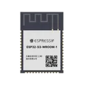
ESP32-S3-WROOM-1-N16R8 is a high-performance Wi-Fi + Bluetooth Low Energy (BLE) module developed by Espressif Systems. It is built around the ESP32-S3 SoC, featuring a dual-core Xtensa LX7 32-bit processor running up to 240 MHz. This module integrates 16 MB Flash memory and 8 MB PSRAM, making it suitable for memory-intensive applications such as AI, image processing, and advanced IoT systems. It also includes an onboard PCB trace antenna, RF circuitry, crystal oscillator, and power management components—allowing designers to quickly integrate wireless connectivity into compact embedded designs. Key Features Processing & Memory Dual-core Xtensa LX7 CPU, up to 240 MHz 384 KB ROM, 512 KB SRAM + 16 KB RTC SRAM 16 MB Flash (Quad SPI) 8 MB PSRAM (Octal/Quad SPI) Connectivity 2.4 GHz Wi-Fi (802.11 b/g/n) Bluetooth 5 (LE) + Mesh support Integrated PCB antenna Peripherals & Interfaces Up to 36 GPIOs Interfaces: UART, SPI, I2C, I2S, PWM, ADC, USB OTG Built-in USB Serial/JTAG support Supports touch sensors, timers, watchdogs, CAN (TWAI) Electrical Characteristics Supply voltage: 3.0 V – 3.6 V TX power: up to ~20.5 dBm RX sensitivity: ~-103.5 dBm Operating temp: −40 °C to +65 °C (typical) Advanced Capabilities Optimized for AI acceleration (vector instructions) Suitable for voice recognition, image processing, and edge AI Low-power modes for battery-operated devices| Typical Applications IoT devices and sensor hubs Smart home & home automation AIoT (voice/image recognition) Industrial automation & monitoring Wearables and health devices USB-connected embedded systems #Module #RF-Transceiver #ESP32-S3
1.9k Uses
5 Stars
AVR series Microcontroller IC 8-Bit 20MHz 32KB (16K x 16) FLASH 32-TQFP (7x7) The ATMEGA328PB-AU is a low-power, high-performance 8-bit AVR microcontroller from Microchip Technology. It is an enhanced version of the widely used ATmega328P, offering additional peripherals while maintaining compatibility. It operates on the AVR RISC architecture, enabling efficient instruction execution with most instructions completed in a single clock cycle. This makes it suitable for embedded systems, industrial control, consumer electronics, and IoT applications. The device comes in a 32-pin TQFP package (AU) and integrates memory, analog features, communication interfaces, and timers into a compact solution. Key Features Core & Performance 8-bit AVR RISC CPU Up to 20 MHz clock frequency Single-cycle instruction execution for high efficiency Memory 32 KB Flash (with self-programming capability) 2 KB SRAM 1 KB EEPROM Peripherals & Interfaces 2 × USART (compared to 1 in ATmega328P) 2 × SPI interfaces 2 × I²C (TWI) interfaces Up to 23 programmable I/O pins Timers & PWM 3 Timers/Counters: 2 × 8-bit timers 1 × 16-bit timer Multiple PWM channels Analog Features 10-bit ADC (up to 8 channels) Analog comparator Power & Voltage Operating voltage: 1.8V to 5.5V Multiple low-power modes: Idle Power-down Power-save Standby Special Features Watchdog Timer with independent oscillator Brown-out Detection (BOD) In-System Programming (ISP) Debug support via debugWIRE Package & Temperature Package: TQFP-32 (AU) Operating temperature: Industrial grade: –40°C to +85°C#CommonPartsLibrary #Microcontroller #Atmega328
667 Uses
2 Stars
PIC PIC® 16F Microcontroller IC 8-Bit 20MHz 14KB (8K x 14) FLASH 40-PDIP The PIC16F877A-I/P is a high-performance 8-bit microcontroller from Microchip Technology, based on a Harvard architecture with separate program and data memory buses. It is designed for a wide range of embedded applications requiring reliable processing, multiple communication interfaces, and analog capability. The device integrates Flash program memory, EEPROM data storage, and numerous peripherals including ADC, timers, serial communication modules, and PWM functions. Packaged in a 40-pin PDIP form factor, it is widely used in industrial automation, consumer electronics, and educational development systems. Core Features 8-bit PIC microcontroller architecture Harvard architecture with RISC instruction set Operating frequency up to 20 MHz Single-cycle instruction execution (except branches) Memory Program Memory: 8K words (Flash) Data Memory (RAM): 368 bytes EEPROM Data Memory: 256 bytes I/O Features Up to 33 programmable I/O pins Multiple input/output ports (PORTA, PORTB, PORTC, PORTD, PORTE) High current sink/source capability on selected pins Analog Features 10-bit Analog-to-Digital Converter (ADC) Up to 8 analog input channels Programmable voltage reference Timers and Control Three timers (Timer0, Timer1, Timer2) Capture/Compare/PWM (CCP) modules Watchdog Timer (WDT) Power-on Reset (POR) and Brown-out Reset (BOR) Communication Interfaces USART (Universal Synchronous/Asynchronous Receiver/Transmitter) SPI (Serial Peripheral Interface) I²C (Inter-Integrated Circuit) via MSSP module Electrical Characteristics Operating Voltage: 4.0V to 5.5V Operating Temperature Range: -40°C to +85°C (Industrial grade) Low power consumption modes available Package Information Package Type: PDIP (Plastic Dual Inline Package) Pin Count: 40 pins Mounting Type: Through-hole Applications Industrial control systems Embedded automation Consumer electronics Sensor interfacing and data acquisition Educational and prototyping platforms #commonpartslibrary #integratedcircuit #microcontroller
867 Uses
2 Stars
ARM® Cortex®-M7 S32K3 Microcontroller IC 32-Bit 160MHz 4MB (4M x 8) FLASH 172-QFP (16x16) S32K344EHT1VPBST is an automotive-grade 32-bit microcontroller from NXP Semiconductors based on the Arm Cortex-M7 core architecture. The device is designed for high-performance real-time automotive body, chassis, powertrain, and domain control applications requiring functional safety, security, and advanced communication interfaces. It integrates high-speed processing capability, extensive peripheral integration, hardware security acceleration, and deterministic control functions suitable for safety-critical embedded systems. The microcontroller operates with an Arm Cortex-M7 CPU core running at high frequency with floating-point support and DSP extensions for computationally intensive applications. Integrated flash memory and SRAM provide embedded program and data storage optimized for automotive embedded control systems. The device supports hardware-assisted security features including secure boot, cryptographic acceleration, and tamper protection for secure automotive network communication and firmware integrity. The S32K344EHT1VPBST includes multiple communication peripherals supporting CAN FD, FlexCAN, LIN, SPI, UART, I2C, and Ethernet interfaces for distributed automotive networking and gateway applications. Advanced analog integration includes ADC modules, timers, PWM generators, watchdogs, and motor-control-oriented peripherals enabling precision sensing and control functionality. The device supports functional safety development aligned with ISO 26262 requirements and includes error correction, memory protection, fault monitoring, and safety management features. Power management functionality supports low-power operating modes for energy-efficient automotive electronic control units. The microcontroller is housed in a thermally enhanced LQFP package suitable for automotive operating environments with extended temperature capability and AEC-Q100 qualification for automotive reliability standards. #commonpartslibrary #integratedcircuit #microcontroller #arm #m7
2 Uses
1 Star
ARM® Cortex®-M4 series Microcontroller IC 32-Bit Single-Core 168MHz 1MB (1M x 8) FLASH 64-LQFP (10x10) Arm® Cortex®-M4 32b MCU+FPU, 210DMIPS, up to 1MB flash/192+4KB RAM, USB OTG HS/FS, Ethernet, 17 TIMs, 3 ADCs, 15 comm. interfaces, and camera Includes ST state-of-the-art patented technology • Core: Arm® 32-bit Cortex®-M4 CPU with FPU, Adaptive real-time accelerator (ART Accelerator) allowing 0-wait state execution from flash memory, frequency up to 168 MHz, memory protection unit, 210 DMIPS/ 1.25 DMIPS/MHz (Dhrystone 2.1), and DSP instructions • Memories – Up to 1 Mbyte of flash memory – Up to 192+4 Kbytes of SRAM including 64- Kbyte of CCM (core coupled memory) data RAM – 512 bytes of OTP memory – Flexible static memory controller supporting CompactFlash™, SRAM, PSRAM, NOR and NAND memories • LCD parallel interface, 8080/6800 modes • Clock, reset, and supply management – 1.8 V to 3.6 V application supply and I/Os – POR, PDR, PVD and BOR – 4-to-26 MHz crystal oscillator – Internal 16 MHz factory-trimmed RC (1% accuracy) – 32 kHz oscillator for RTC with calibration – Internal 32 kHz RC with calibration • Low-power operation – Sleep, Stop, and Standby modes –VBAT supply for RTC, 20×32-bit backup registers + optional 4 KB backup SRAM • 3×12-bit, 2.4 MSPS A/D converters: up to 24 channels and 7.2 MSPS in triple interleaved mode • 2×12-bit D/A converters • General-purpose DMA: 16-stream DMA controller with FIFOs and burst support • Up to 17 timers: up to twelve 16-bit and two 32- bit timers up to 168 MHz, each with up to 4 IC/OC/PWM or pulse counter and quadrature (incremental) encoder input • Debug mode – Serial wire debug (SWD) & JTAG interfaces – Cortex-M4 Embedded Trace Macrocell™ • Up to 140 I/O ports with interrupt capability – Up to 136 fast I/Os up to 84 MHz – Up to 138 5 V-tolerant I/Os • Up to 15 communication interfaces – Up to 3 × I2C interfaces (SMBus/PMBus) – Up to 4 USARTs/2 UARTs (10.5 Mbit/s, ISO 7816 interface, LIN, IrDA, modem control) – Up to 3 SPIs (42 Mbits/s), 2 with muxed full-duplex I2S to achieve audio class accuracy via internal audio PLL or external clock – 2 × CAN interfaces (2.0B Active) – SDIO interface • Advanced connectivity – USB 2.0 full-speed device/host/OTG controller with on-chip PHY – USB 2.0 high-speed/full-speed device/host/OTG controller with dedicated DMA, on-chip full-speed PHY and ULPI – 10/100 Ethernet MAC with dedicated DMA: supports IEEE 1588v2 hardware, MII/RMII #commonpartslibrary #integratedcircuit #microcontroller
52 Uses
1 Star
The NE555 devices are precision timing circuits capable of producing accurate time delays or oscillation. In time-delay or monostable operating modes, the timed interval is controlled by a single external resistor and capacitor network. In the astable mode of operation, the frequency and duty cycle are controlled independently with two external resistors and a single external capacitor. Each timer has a trigger level equal to approximately one-third of the supply voltage and a threshold level equal to approximately two-thirds of the supply voltage. These levels can be altered by use of the control voltage pin (CONT). When the trigger input (TRIG) is less than the trigger level, the flip-flop is set and the output goes high. If TRIG is greater than the trigger level and the threshold input (THRES) is greater than the threshold level, the flip-flop is reset and the output is low. The reset input (RESET) overrides all other inputs and is used to initiate a new timing cycle. If RESET is low, the flip-flop is reset and the output is low. Whenever the output is low, a lowimpedance path is provided between the discharge pin (DISCH) and the ground pin (GND). Tie all unused inputs to an appropriate logic level to prevent false triggering. The output circuit is capable of sinking or sourcing current up to 200mA. Operation is specified for supplies of 5V to 15V. With a 5V supply, output levels are compatible with TTL inputs. Features - Timing from microseconds to hours - Astable or monostable operation - Adjustable duty cycle - TTL-compatible output can sink or source up to 200mA - On products compliant to MIL-PRF-38535, all parameters are tested unless otherwise noted. Applications - Pulse-shaping circuits - Missing-pulse detectors - Pulse-width modulators - Pulse-position modulators - Sequential timers - Pulse generators -F requency dividers - Industrial controls
2.3k Uses
1 Star
Bluetooth, WiFi 802.11b/g/n, Bluetooth v5.0 Transceiver Module 2.4GHz PCB Trace Surface Mount The ESP32-C3-WROOM-02-N4 is a compact, general-purpose Wi-Fi and Bluetooth Low Energy (BLE) module developed by Espressif Systems. It is built around the ESP32-C3 SoC and integrates RF components, crystal oscillator, flash memory, and PCB antenna in a single module. It is designed for a wide range of applications such as IoT devices, smart home systems, industrial automation, and consumer electronics, offering a balance of performance, low power consumption, and cost efficiency. Key Features MCU & Memory 32-bit RISC-V single-core processor up to 160 MHz 384 KB ROM 400 KB SRAM + 8 KB RTC SRAM Integrated 4 MB SPI flash (N4 variant) Connectivity 2.4 GHz Wi-Fi (802.11 b/g/n) Supports Station, SoftAP, and Station + SoftAP modes Bluetooth 5 (BLE) with mesh support Data rates up to 150 Mbps (Wi-Fi) Peripherals & Interfaces Up to 15 GPIOs Interfaces: SPI, UART, I2C, I2S LED PWM ADC (SAR) Timers & watchdog USB Serial/JTAG support TWAI® (CAN 2.0 compatible) #commonpartslibrary #transceiver #module #wireless #rf
664 Uses
1 Star
The CH32X035/X033 series, developed by WCH, encompasses industrial-grade microcontrollers based on the QingKe RISC-V core. These microcontrollers, including models such as the CH32X035R8T6, CH32X035C8T6, CH32X035G8U6, CH32X035G8R6, CH32X035F8U6, CH32X035F7P6, and CH32X033F8P6, are equipped with integrated USB and PD PHY, supporting USB Host and Device functionalities, as well as PDUSB and Type-C fast charging capabilities. The series features a programmable protocol I/O controller, two groups of operational amplifiers (OPA), three groups of comparators (CMP), four USARTs, I2C, SPI, multiple timers, a 12-bit ADC, and 14-channel capacitive touch-key interfaces, among other peripherals. These microcontrollers offer a comprehensive suite of features, including a 32-bit QingKe RISC-V4C core with support for the RV32IMAC instruction set, fast interrupt handling, and low-power modes, making them suitable for a wide range of embedded applications. With a robust memory architecture comprising 20KB SRAM and 62KB CodeFlash, alongside various power management and security features, the CH32X035/X033 series is designed to deliver high performance and flexibility for industrial applications.
5 Uses
1 Star
The TPL5110 Power Timer is a stand-alone breakout that will turn any electronics into low-power electronics! It will take care of turning your project on/off using a built in timer that can vary from once-every 100ms up to once every two hours. Basically, the TPL will turn on periodically, adjustable by potentiometer or resistor, and turn on your project's power. It will then wait until a signal is received from the project to tell the TPL that it can safely turn off the power. If the TPL does not receive a signal by the set time-out, it will reset the device like a watchdog timer. #Sublayout #Module #PowerTimer #TPL5110
10 Uses
1 Star
QFP80P1600X1600X120-64N https://ww1.microchip.com/downloads/en/DeviceDoc/atmegas128_ds.pdf Rad-Tol 8-bit AVR Microcontroller, 3.3V, 8 MHz with 128 KB Flash, 4 KB EEPROM, 4 KB SRAM, 10-bit ADC, TWI, RTC, 16-bit PWM, USART, SPI and 16-bit Timer/Counter 1.2 Microchip ATMEGAS128-MD-HP N/A https://www.mouser.co.uk/ProductDetail/Microchip-Technology/ATMEGAS128-MD-HP?qs=sPbYRqrBIVk98zCv1OqHjw%3D%3D
81 Uses
1 Star