Interface ICs
An interface IC is a type of integrated circuit that is designed to facilitate communication between two devices or systems. These devices are commonly used in electronic systems to enable the transfer of data and control signals between different components or subsystems. Some common use cases for interface ICs include connecting microcontrollers to peripherals such as sensors or displays, linking multiple processors together in a network, and enabling communication between devices using different communication protocols. Flux.ai has the world's largest community-driven public library of interface ICs, with footprints, symbols, datasheets, and simulation models. This library is a valuable resource for engineers and designers who need access to accurate and up-to-date information on these important components. Whether you are working on a new design project or simply looking to learn more about interface ICs, Flux.ai is an excellent resource to help you find the information you need.
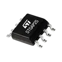
M24256E-FMN6TP
EEPROM Memory IC 256Kbit I2C 1 MHz 450 ns 8-SO The M24256E-FMN6TP is a 256-Kbit (32 Kbyte) I²C-compatible serial EEPROM from STMicroelectronics. It is designed for reliable, non-volatile data storage in a wide range of electronic applications including consumer, industrial, and automotive systems. The device supports standard (100 kHz), fast (400 kHz), and fast-mode plus (1 MHz) I²C communication, enabling efficient data transfer. It features byte and page write operations, low power consumption, and a high endurance of write cycles, making it suitable for frequent data logging and configuration storage. Housed in a compact SO8 package, the device is optimized for space-constrained PCB designs while maintaining robust performance and data retention capabilities. Key Features Memory size: 256 Kbit (32 Kbyte) Interface: I²C (2-wire serial interface) Clock frequency: Standard mode: 100 kHz Fast mode: 400 kHz Fast-mode Plus: 1 MHz Supply voltage range: 1.7 V to 5.5 V Page write capability: up to 64 bytes Write cycle time: ~5 ms (typical) Data retention: > 200 years Endurance: > 4 million write cycles Hardware write protection available ESD protection and latch-up immunity Functional Description The device operates as a slave on the I²C bus and supports: Byte write and read Page write (up to 64 bytes) Random and sequential read operations Memory addressing is internally managed using a 16-bit address pointer, allowing access to the full 32 KB memory array. The device includes an internal write cycle controller, eliminating the need for external timing management. Pin Configuration (SO8 Package) A0, A1, A2: Device address inputs VSS: Ground SDA: Serial data line SCL: Serial clock line WC: Write control (hardware write protection) VCC: Supply voltage Absolute Maximum Ratings Supply voltage (VCC): -0.3 V to 6.5 V Input voltage: -0.3 V to VCC + 0.6 V Storage temperature: -65°C to +150°C Operating temperature (industrial grade): -40°C to +85°C Electrical Characteristics Low standby current: < 1 µA (typical) Operating current: < 1 mA Input/output compatible with CMOS logic levels Schmitt trigger inputs for noise immunity Timing Characteristics Write cycle time: 5 ms (typical) Fast-mode Plus support up to 1 MHz Sequential read supports continuous data streaming Package Information Package type: SO8 (8-lead Small Outline) Mounting: Surface-mount (SMD) Tape & reel packaging (TP suffix) Applications Configuration storage Calibration data storage Data logging systems Industrial control systems Consumer electronics Embedded systems requiring non-volatile memory Advantages High endurance and long data retention Wide voltage range (ideal for mixed-voltage systems) Compact footprint High-speed I²C compatibility (up to 1 MHz) #commonpartslibrary #integratedcircuit #memory
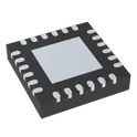
14 Uses0 StarsAFE881H1RRUR
2 Channel AFE 16 Bit 24-UQFN (4x4) The AFE881H1RRUR is a highly integrated analog front-end (AFE) designed for multi-channel data acquisition systems. It combines precision analog signal conditioning with high-speed analog-to-digital conversion, making it suitable for applications such as medical instrumentation, industrial measurement, and test and measurement equipment. The device integrates low-noise amplifiers, programmable gain stages, anti-aliasing filters, and high-resolution ADCs into a compact package, reducing system complexity and board space. Key Features Multi-channel analog front-end integration High-resolution analog-to-digital conversion Low-noise input stage for precision measurements Programmable gain amplifier (PGA) Integrated anti-aliasing filters High sampling rate capability Serial digital interface (SPI-compatible) Low power consumption for portable systems Compact surface-mount package Electrical Characteristics (Typical – refer to datasheet for exact values) Supply Voltage: ~1.8 V to 3.3 V (analog/digital domains) Input Voltage Range: Dependent on configuration Resolution: Up to 16-bit or higher (device dependent) Sampling Rate: Up to several MSPS (depending on mode) Power Consumption: Optimized for performance/power balance Functional Blocks Low-noise input buffer Programmable gain amplifier (PGA) Anti-aliasing filter High-speed ADC core Digital control interface (SPI) Clock management circuitry Package Information Package Type: QFN / VQFN (exact variant per TI RRU package code) Mounting Type: Surface Mount Pin Count: Typically 40+ pins (refer to datasheet for exact count) Applications Medical imaging and instrumentation Industrial data acquisition systems Oscilloscopes and test equipment Communication systems Precision sensor interfaces Advantages High integration reduces external components Improved signal integrity due to low-noise design Flexible configuration via programmable gain Compact footprint for dense PCB layouts Notes Exact electrical parameters, pin configuration, and performance metrics must be verified in the official Texas Instruments datasheet. Proper PCB layout (grounding, shielding, and decoupling) is critical for optimal performance. #commonpartslibrary #integratedcircuit
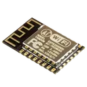
1 Uses0 StarsESP-12F
WiFi 802.11b/g/n Transceiver Module 2.4GHz ~ 2.5GHz Integrated, Trace Surface Mount The ESP-12F is a compact WiFi module based on the ESP8266EX, widely used in IoT and embedded systems due to its low cost and built-in networking capabilities. Integrated WiFi (2.4 GHz) Supports 802.11 b/g/n Built-in TCP/IP stack (no external WiFi processor needed) Microcontroller + WiFi in one Powered by the ESP8266EX SoC Can run user applications directly (not just a WiFi modem) Flash Memory Typically 4 MB SPI flash (varies by version) GPIO Support Multiple multifunction pins: Digital I/O PWM I2C SPI UART ADC (1 channel) Size: ~16 mm × 24 mm Mounting: Castellated SMD module Antenna: Built-in PCB trace antenna (requires proper keepout zone) Power Requirements Operating Voltage: 3.0V – 3.6V (typical 3.3V) Current Consumption: Idle: ~70 mA Peak (TX): up to ~300 mA Common Interfaces UART – programming and debugging SPI – peripheral communication I2C (software-based) GPIO – general-purpose control #commonpartslibrary #transceiver #module #wireless #rf #wifi
183 Uses0 StarsSIM7600E-H
Cellular EDGE, GPRS, GSM, HSPA+, LTE, UMTS Transceiver Module 900MHz, 1.8GHz Antenna Not Included Surface Mount The SIM7600E-H is a multi-mode LTE module that supports: LTE (4G) Cat-4 with up to 150 Mbps download / 50 Mbps upload 3G (UMTS/HSPA+) 2G (GSM/GPRS/EDGE) fallback for global network compatibility It is built in a compact SMT/LCC package (about 30 × 30 mm) and is widely used for embedded devices that need mobile internet and GNSS positioning Key Features Network support LTE-FDD / LTE-TDD (global bands depending on variant) UMTS/HSPA+ GSM/GPRS/EDGE fallback Data speed LTE Cat-4: up to 150 Mbps downlink 3G/2G fallback for lower-speed connectivity GNSS built-in GPS / GLONASS / other satellite positioning support Interfaces USB 2.0 UART GPIO I2C ADC PCM (audio support) SIM card interface Software / protocols AT command control TCP/IP, UDP, HTTP, HTTPS, FTP, DNS Driver support for Windows, Linux, Android Power supply ~3.4V to 4.2V typical operating range Operating temperature -40°C to +85°C (industrial grade) Typical Applications IoT devices GPS trackers Smart metering Industrial routers / gateways Remote monitoring systems Vehicle telematics Point-of-sale terminals #commonpartslibrary #rf #wireless #transceiver #module
223 Uses0 StarsADAQ7767-1BBCZ
+/-24V PGA I/P 24-BIT 256KSPS DA The ADAQ7767-1BBCZ is a high-performance, precision data acquisition (DAQ) µModule® system from Analog Devices. It integrates a 24-bit sigma-delta analog-to-digital converter (ADC), signal conditioning, and essential analog front-end components into a compact package. Designed for high accuracy and ease of use, it significantly reduces design complexity, layout effort, and noise sensitivity in precision measurement systems. This device is optimized for applications requiring high resolution, low noise, and excellent DC performance, such as industrial automation, instrumentation, and test equipment. Key Features 24-bit resolution sigma-delta ADC Integrated analog front end (AFE) Low noise, high dynamic range performance Programmable gain amplifier (PGA) Wide input bandwidth Low drift and high linearity SPI-compatible serial interface Internal reference and buffer options Compact system-in-package (SiP) design Electrical Characteristics Resolution: 24 bits Sampling Rate: Up to 256 kSPS (depending on configuration) Input Type: Differential Input Voltage Range: ±VREF (dependent on configuration) Signal-to-Noise Ratio (SNR): ~108 dB (typical) Total Harmonic Distortion (THD): Low distortion performance Reference Voltage: Internal or external supported Power Requirements Analog Supply Voltage (AVDD): 4.5 V to 5.5 V (typical) Digital Supply Voltage (DVDD): 1.8 V to 3.3 V Power Consumption: Optimized for precision applications Interface Communication: SPI-compatible serial interface Data Output: Serial digital output Control: Register-based configuration Package Information Package Type: µModule® (BGA) Package Code: BBCZ Mounting Type: Surface mount Compact footprint for space-constrained designs Operating Conditions Operating Temperature Range: -40°C to +85°C (industrial grade) Storage Temperature Range: -65°C to +150°C Applications Industrial process control Data acquisition systems Precision instrumentation Test and measurement equipment Medical instrumentation Energy monitoring systems Advantages Reduces PCB design complexity Minimizes noise and parasitic effects Factory-optimized signal chain performance Faster time-to-market
1 Uses0 StarsLBES5PL2EL-923
802.15.4, Bluetooth, WiFi 802.11a/b/g/n/ac/ax, Bluetooth v5.3, Zigbee® Transceiver Module 2.4GHz, 5GHz Antenna Not Included, U.FL/MHF, PCB Trace Surface Mount The LBES5PL2EL-923 is a compact, low-power Bluetooth® Low Energy (BLE) module developed by Murata. It integrates a Nordic Semiconductor SoC (nRF52 series) with an onboard antenna, providing a complete RF solution for wireless connectivity in embedded systems. The module is designed for IoT, wearable, and low-power wireless applications, offering reliable communication, small footprint, and minimal external component requirements. Key Features Integrated Bluetooth® Low Energy (BLE) 5.x compliant module Based on Nordic Semiconductor nRF52 series SoC Built-in chip antenna (no external antenna required) Ultra-low power consumption suitable for battery-powered devices Integrated RF matching and shielding Supports multiple BLE roles (Central, Peripheral, Broadcaster, Observer) Compact surface-mount package Pre-certified RF module (reduces certification effort) Electrical Characteristics Supply Voltage Operating Voltage: 1.7 V to 3.6 V Current Consumption TX Mode: ~5–10 mA (depending on output power) RX Mode: ~5 mA Sleep Mode: < 2 µA RF Characteristics Frequency Band: 2.4 GHz ISM (2400–2483.5 MHz) Output Power: up to +4 dBm Sensitivity: approx. -96 dBm Interfaces UART SPI I²C (TWI) GPIO (multiplexed) ADC inputs PWM Mechanical Specifications Package Type: Surface Mount Module (SMD) Dimensions: ~10 mm × 7 mm × 1.4 mm (approx.) Integrated antenna and shielding Environmental Ratings Operating Temperature: -40°C to +85°C Storage Temperature: -40°C to +125°C Compliance & Certifications Bluetooth SIG qualified FCC / IC / CE (module-level certification, varies by variant) RoHS compliant Applications IoT devices Wearables Smart home products Wireless sensors Industrial monitoring systems Pin Configuration (Summary) Power: VDD, GND Communication: UART, SPI, I²C GPIOs: Configurable digital I/O RF: Integrated antenna (no RF pin required) Design Considerations Follow recommended PCB layout for antenna clearance Avoid copper under antenna region Provide stable power supply with proper decoupling capacitors Ensure proper grounding for RF performance #commonpartslibrary #integratedcircuit #transceiver #wireless #rf
15 Uses0 StarsPEC06SAAN
Connector Header Through Hole 6 position 0.100" (2.54mm) The PEC06SAAN is a compact, low-cost incremental rotary encoder manufactured by Bourns. It is designed for user interface applications requiring precise rotational input, such as volume controls, menu navigation, and position sensing. This encoder provides reliable quadrature output signals and is suitable for through-hole PCB mounting. Its robust mechanical design ensures long operational life and consistent performance in consumer and industrial electronics. Key Features Incremental (relative) rotary encoder Compact, space-saving design Through-hole mounting configuration Quadrature output (A and B channels) Optional integrated push switch (depending on variant) Detent and non-detent options available High reliability with long rotational life RoHS compliant Electrical Characteristics Supply voltage: Typically 5 VDC (logic-level output) Output type: Digital quadrature (A/B signals) Contact resistance: ≤ 100 mΩ Insulation resistance: ≥ 100 MΩ @ 250 VDC Dielectric strength: 300 VAC for 1 minute Mechanical Characteristics Rotation type: Incremental Number of pulses per revolution (PPR): Typically 6 to 24 (variant dependent) Detent positions: Variant dependent Rotational torque: 10 to 70 gf·cm (typical range) Shaft length: Varies by suffix (e.g., 15 mm typical) Shaft type: Knurled or D-cut (variant dependent) Mounting type: Through-hole PCB Terminal type: PC pins Environmental Specifications Operating temperature range: −30°C to +70°C Storage temperature range: −40°C to +85°C Humidity: Up to 85% RH (non-condensing) Mechanical Life Rotational life: Up to 30,000 cycles (typical) Physical Dimensions Body size: Approximately 12 mm × 11 mm × 5 mm (excluding shaft) Shaft diameter: Typically 6 mm Pin pitch: Standard 2.54 mm Applications Consumer electronics (audio controls, appliances) Industrial control panels Embedded systems and microcontroller interfaces Automotive user interfaces Instrumentation and test equipment #commonpartslibrary #connector #header
28 Uses0 StarsECMF2-40A100N6
2 Line Common Mode Choke Surface Mount 100mA DCR 3Ohm (Typ) , -55C ~ 125C The ECMF2-40A100N6 and ECMF4-40A100N10 are highly integrated common mode filters designed to suppress EMI/RFI common mode noise on high speed differential serial buses like HDMI 2.1, HDMI 2.0, HDMI1.4, USB4, USB 3.2 Gen 2, USB 2.0, ethernet, MIPI, Display Port and other high speed serial interfaces. They have a very large differential bandwidth to comply with these standards and can also protect and filter one or two differential lanes. 10.7 GHz differential bandwidth to comply with HDMI 2.1, HDMI 2.0, HDMI 1.4, USB4, USB 3.2 Gen2, USB 2.0, MIPI, Display port 2.0, etc. • High common mode attenuation on WLAN frequencies: – -15 dB at 2.4 GHz – -21 dB at 5.0 GHz – -17 dB at 6.0 GHz • Low serial resistance: 3.0 Ω • Very low PCB space consumption • Thin package: 0.5 mm max. • High reduction of parasitic elements through integration • Lead free and RoHS package • Exceeds IEC 61000-4-2 level 4 standard: – Contact discharge: ◦ ±9 kV (contact discharge, ECMF2-40A100N6) ◦ ±10 kV (contact discharge, ECMF4-40A100N10) – Air discharge: ◦ ±20 kV (air discharge, ECMF2-40A100N6) ◦ ±25 kV (air discharge, ECMF4-40A100N10)
18 Uses0 Stars