Interface ICs
An interface IC is a type of integrated circuit that is designed to facilitate communication between two devices or systems. These devices are commonly used in electronic systems to enable the transfer of data and control signals between different components or subsystems. Some common use cases for interface ICs include connecting microcontrollers to peripherals such as sensors or displays, linking multiple processors together in a network, and enabling communication between devices using different communication protocols. Flux.ai has the world's largest community-driven public library of interface ICs, with footprints, symbols, datasheets, and simulation models. This library is a valuable resource for engineers and designers who need access to accurate and up-to-date information on these important components. Whether you are working on a new design project or simply looking to learn more about interface ICs, Flux.ai is an excellent resource to help you find the information you need.
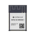
ESP32-S3-WROOM-1-N16R8
Bluetooth, WiFi 802.11b/g/n, Bluetooth v5.0 Transceiver Module 2.4GHz PCB Trace Surface Mount The ESP32-S3-WROOM-1-N16R8 is a high-performance Wi-Fi + Bluetooth Low Energy (BLE) module developed by Espressif Systems. It is built around the ESP32-S3 SoC, featuring a dual-core Xtensa LX7 32-bit processor running up to 240 MHz. This module integrates 16 MB Flash memory and 8 MB PSRAM, making it suitable for memory-intensive applications such as AI, image processing, and advanced IoT systems. It also includes an onboard PCB trace antenna, RF circuitry, crystal oscillator, and power management components—allowing designers to quickly integrate wireless connectivity into compact embedded designs. Key Features Processing & Memory Dual-core Xtensa LX7 CPU, up to 240 MHz 384 KB ROM, 512 KB SRAM + 16 KB RTC SRAM 16 MB Flash (Quad SPI) 8 MB PSRAM (Octal/Quad SPI) Connectivity 2.4 GHz Wi-Fi (802.11 b/g/n) Bluetooth 5 (LE) + Mesh support Integrated PCB antenna Peripherals & Interfaces Up to 36 GPIOs Interfaces: UART, SPI, I2C, I2S, PWM, ADC, USB OTG Built-in USB Serial/JTAG support Supports touch sensors, timers, watchdogs, CAN (TWAI) Electrical Characteristics Supply voltage: 3.0 V – 3.6 V TX power: up to ~20.5 dBm RX sensitivity: ~-103.5 dBm Operating temp: −40 °C to +65 °C (typical) Advanced Capabilities Optimized for AI acceleration (vector instructions) Suitable for voice recognition, image processing, and edge AI Low-power modes for battery-operated devices| Typical Applications IoT devices and sensor hubs Smart home & home automation AIoT (voice/image recognition) Industrial automation & monitoring Wearables and health devices USB-connected embedded systems #Module #RF-Transceiver #ESP32-S3
2.1k Uses5 Stars
Page 1 of 189
Next