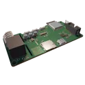
Patient Ivory Interocitor
Introducing our innovative modular, AI-powered DIY laptop carrier board project! This design focuses on a step-by-step approach, starting with a solid architectural scaffold that lays the groundwork for a high-performance system. The project is built around a hierarchical schematic structure including: • A Top Sheet outlining the system overview and power tree • SoM Connectors organized into three 100-pin assemblies (two CM4/5-compatible and one dedicated to high-speed operation) • Dedicated Power/PD management • An M.2 A+E interface for the Coral TPU (PCIe x1 from PORT0) • An M.2 M-key interface for an NVMe SSD (PCIe x2 from PORT1) • Comprehensive USB & Hub configurations • A microSD integration module • Supervisory and Reset controls The design aligns with cost-effective 4-layer board stackup practices (JLCPCB friendly) while following best high-speed design guidelines for USB/PCIe integrity. The integrated silkscreen placeholders feature custom sci-fi fonts for a unique, personal branding touch. Key routing notes include precise PCIe lane mappings based on the Orange Pi CM5 manual, ensuring clean ground return paths, effective decoupling, and proper AC-coupling placement. With paired USB hubs optimized for minimal depth and latency and robust power sequencing strategies, this project is poised to evolve into a high-speed, scalable prototype. #DIYElectronics #ModularDesign #PCBDesign #EmbeddedSystems #PCIe #USBDesign #OrangePiCM5 #TechInnovation #HighSpeedElectronics... show more0 Uses
0 Comments
0 Stars
Black Magick Heavy Industries - KYB1 aca5
Black Magick Heavy Industries KYB1 programmable wireless keyboard, model BLKMGK-KYB1-BASIC, featuring a 69-key layout, XIAO ESP32-C5 controller, Seeed Studio Wio-SX1262 LoRa/Wi-Fi module, configurable RGB backlighting, microSD storage, dual USB-C interface... show more0 Uses
0 Comments
0 Stars
Black Magick Heavy Industries - KYB1
Black Magick Heavy Industries KYB1 programmable wireless keyboard, model BLKMGK-KYB1-BASIC, featuring a 69-key layout, XIAO ESP32-C5 controller, Seeed Studio Wio-SX1262 LoRa/Wi-Fi module, configurable RGB backlighting, microSD storage, dual USB-C interface... show more0 Uses
0 Comments
0 Stars
Coffee Waker Main HQ W/ Module V5.0.1 1243 f1b0 4389
Multi-subsystem ESP32-S3 coffee maker/alarm controller board for a Coffee Waker appliance. The design uses an ESP32-S3-WROOM-1-N8R8 module as the main Wi-Fi/Bluetooth MCU, with USB-C 2.0 device connectivity through a USB4105-GF-A connector, 5.1 kΩ CC pull-downs, and USBLC6-2SC6 ESD protection on the USB D+/D− pair. Power architecture includes a 12 V input on a JST VH B4P connector, a TPS62932 buck regulator generating the 5 V rail, a TLV1117LV33 3.3 V LDO for MCU/logic power, and TPS22919 load switches for controlled 3.3 V/5 V peripheral rails. Functional blocks include an NAU7802 load-cell ADC on I2C with two differential load-cell channels, a MAX98357A I2S audio amplifier/DAC with speaker/output filtering, a microSD socket on SDIO, I2C/test headers, UART/programming header, and auxiliary JST VH connectors for wake-light or external loads. The high-voltage section includes 120 VAC input/output screw terminals, a 5 V SPST-NO relay rated 15 A / 240 VAC max, a 1 A fuse, MOV surge suppression, diode snubber, and a dedicated heater output terminal.... show more0 Uses
0 Comments
0 Stars
P-001_AnandKumar_IOTSentinels
This Gerber file contains the necessary information for fabricating the PCB design of a Bluetooth-enabled headphone. The design includes multiple layers, showcasing the electrical connections and component placements on both the top and bottom layers. Top Layer (Copper traces and components): The top copper layer is primarily responsible for routing the signals from key components such as the ESP32 module, MAX98357A audio amplifier, and the microphone. The ESP32 module, responsible for Bluetooth communication, is positioned centrally to optimize signal flow and minimize interference. Decoupling capacitors (100nF) are placed near critical components to ensure signal stability and noise suppression. Audio signal paths, as well as power distribution, are carefully routed to prevent cross-talk and ensure high-quality sound. Bottom Layer (Copper traces): The bottom layer contains the ground plane and additional routing for power and signal connections. The charging module (TP4056) and voltage regulator (AMS1117) are placed to manage power distribution, ensuring stable battery charging and regulated output for the ESP32 and other components. Connections to external interfaces such as the MicroSD breakout and auxiliary input are routed efficiently to avoid conflicts. Additional Components: All critical components are labeled, including decoupling capacitors (100nF) and resistors where needed, as well as external interfaces like the MicroSD card breakout. Mounting holes are provided for secure installation in a headphone casing, ensuring the board can be integrated seamlessly into the final product. The PCB is designed to minimize noise, with short signal paths and proper grounding for high-fidelity audio performance. This Gerber file ensures accurate manufacturing by containing data for copper layers, silkscreen, solder mask, and drill files.... show more0 Uses
23 Comments
0 Stars