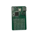
Explain this project. Describe its purpose, core...

Explain this project.
Describe its purpose, core components, and how they interact.
Break down the design, implementation, and functionality. Highlight key technologies, dependencies, and design choices, including trade-offs and optimizations.
Discuss potential challenges, performance considerations, and real-world applications. If applicable, suggest areas for improvement, scalability, and future enhancements.
add 5V charge solution

add 5V charge solution
2y
5
add level shifters to I2C lines

Ref
Image

Image

https://cdn-learn.adafruit.com/assets/assets/000/113/060/original/adafruit_products_schem.png?1657549240
2y
add level shifters to I2C lines
2y
4
Ref for Level Shifters: img

Ref for Level Shifters:
img

Image

2y
6
use this in conjunction with https://www.adafruit.com/product/5434

there is no official pinout for this part. Pick whatever works best for you and use jumper wires to route them to the corresponding programming pins.
For this project, Mode 1 is the SPI bus which allows you to flash the bootloader onto the Atmega328.
Mode 2 is the UART bus which allows you to communicate with it.
2y
2y
3
Note to self: purchase a bunch of 1.27mm headers

Note to self: purchase a bunch of 1.27mm headers
2y
1
Check that all reset/enable have an external pull-up or pull-down resistors for ...

@copilot Check that all reset/enable have an external pull-up or pull-down resistors for U2. Report action items in an ordered list.
2y
From the project components and the netlist, it appears that there isn't an external resistor connected to the LSM6DS3TR-C (U2) for either a pull-up or pull-down functionality. The LSM6DS3TR-C doesn't have a dedicated reset or enable pin, but the pins most likely to require a pull-up or pull-down resistor are the SDX, SCX, and CS pins.
Based on this information, the following actions should be taken:
  1. Examine the data sheet for LSM6DS3TR-C to verify the necessity of pull-up or pull-down resistors on these pins.
  2. Confirm if the MCU used in the design has built-in pull-up or pull-down resistors and whether they are being used.
  3. If pull-up or pull-down resistors are required, calculate the required resistance values using Ohm's law and the properties of the circuit.
  4. Add the required external pull-up/pull-down resistors connecting to the pins of interest (SDX, SCX, and CS) in the schematic using suitable designators, then update the netlist.
  5. Evaluate the updated circuit for performance – ensure correct operation of the LSM6DS3TR-C and verify communication with the rest of the circuit.
  6. Repeat these steps for all other devices that may require pull-up or pull-down resistors, following each device's specific requirements from the data sheet.
2y
9
Check that all reset/enable have an external pull-up or pull-down resistors. Rep...

@copilot Check that all reset/enable have an external pull-up or pull-down resistors. Report action items in an ordered list.
2y
Based on the provided project description, there appears to be a reset signal associated with the Designator MCU_RESET. The relevant parts connected to it are MCU_RESET:P1, J1:9, and J1:2.
However, the project description and component information does not provide precise details about whether a pull-up or pull-down resistor is attached to the reset pin of these connected parts.
Here are the steps to check that:
  1. Examine the Schematic: The schematic needs to be examined to check if a pull-up or pull-down resistor is connected to the reset pin of the devices associated with MCU_RESET.
  2. Check MCU_RESET label in Circuit: Given MCU_RESET is connected to MCU_RESET:P1, J1:9, and J1:2, it would be prudent to investigate more about “P1, 9, and 2”, i.e. whether these point to reset pins on the microcontroller and the other device (J1).
  3. Consult Component Datasheets: It's also recommended to consult the component datasheets specified in the properties section of each designator (if available) to verify whether an external pull-up or pull-down resistor is necessary for the reset/enable pin.
  4. Make Necessary Changes: Based on these observations, if needed, add pull-up or pull-down resistors as required to the reset/enable pins on the schematic.
Remember, these steps are general approaches and the specific actions may vary depending on the exact requirement and constraints of the project and components.
You may also need more contextual information like schematics, board layout, and specifications of these parts connected to this signal to draw more definitive conclusions.
Source(s):
2y
8
IMU_SCL
C7
Capacitance
1uF
IMU_INT2
IMU_INT1
IMU_SCL
C8
Capacitance
100nF
MCU_SDA
IMU_SDA
C6
Capacitance
1uF
IMU_INT1
IMU_SDA
MCU_SCL
IMU_SCL
Q1
3V3
+5V
3V3
+3V3
+3V3
R4
Resistance
Resistance
J2
U1
U2
End of Life


No results...

8x8 Display with IMU V2

8x8 Display with IMU V2 thumbnail
Mixed Voltage Arduino Nano Integration Example on a 4 Layer PCB
Changelog/TODO: -Breakout the SPI Bus in a 2.54mm header in a snap off manner -add an IMU -Reorder the rows of the LEDs

Pricing & Availability

Distributor

Qty 1

Arrow

$12.80–$13.76

Digi-Key

$23.83

LCSC

$10.50

Mouser

$25.78

Verical

$0.01–$0.02

Controls