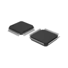
STM32L151RCT6 Project Overview
Thought for 3 mins 18 sec
Here’s a clear overview of this project and how to take it forward.
What this project is
- It is a pin-breakout schematic for the STM32 ultra‑low‑power MCU family, centered on STM32L151RCT6 in LQFP‑64 (10 x 10 mm, 0.5 mm pitch).
- Every package pin is represented as an individual pin breakout on the schematic (no nets yet). Power, reset, boot, clock, and GPIO pins are exposed for integration into a full design.
Core device and key specs (from the Datasheet)
- CPU: ARM Cortex‑M3, up to 32 MHz max.
- Supply range: with BOR enabled at power‑on, 1.8 to 3.6 V (1.65 to 3.6 V if BOR disabled; see datasheet for exact conditions).
- Low‑power features: ultra‑low currents in Stop/Standby; dynamic voltage scaling; several low‑power modes (Sleep, Low‑power run/sleep, Stop w/wout RTC, Standby w/wout RTC). Typical figures include 0.29 µA Standby (RTC off), about 1.15 µA Standby + RTC, and about 185 µA/MHz in Run mode (conditions per datasheet tables).
- Package: LQFP‑64, 10 x 10 mm, 0.5 mm pitch.
- Boot modes: Boot from Flash, System memory (UART/USB bootloader), or RAM via BOOT pins.
- Clocks: HSE on PH0-OSC_IN/PH1-OSC_OUT; LSE 32.768 kHz on PC14-OSC32_IN/PC15-OSC32_OUT.
- Analog supply: VDDA/VSSA. Recommended to power VDDA from the same source as digital VDD; tolerance between VDD and VDDA per datasheet (max 300 mV during power‑up, 140 mV in operation). ADC requires at least 1.8 V on VDDA.
- LCD note: The datasheet specifies that the integrated LCD controller is present “except STM32L151xC devices.” Since STM32L151RCT6 is an L151xC device, it does not include the LCD step‑up/segment driver. If a VLCD terminal appears in this symbol, treat it as not used for this specific MCU.
- Reference: 2301101230_STMicroelectronics-STM32L151RCT6_C124721.pdf.
How the schematic is structured (and how things interact in a complete design)
- Power and grounds: Multiple digital VDD/VSS pins plus VDDA/VSSA for analog. In a real design, each VDD/VSS pair needs local decoupling; VDDA typically gets its own decoupling and often a small RC/ferrite bead filter from the 3V3 rail.
- Reset and boot: NRST (reset) and BOOT0 determine startup behavior. BOOT0 normally needs a pull‑down to ensure boot from Flash by default (datasheet/Application Note AN2606 cover options).
- Debug/programming: SWD uses PA13 (SWDIO) and PA14 (SWCLK) which are shared with JTAG signals. Plan for a 2×5/1×6 programming header and keep those pins accessible during manufacturing.
- Timing: The MCU can run from its internal RCs; add crystals if you need precise system timing (HSE) or accurate RTC (LSE) on the pins above.
- IO: All other PAx/PBx/PCx/PDx terminals are the MCU GPIO/peripheral pins; they remain unconnected for the integrator to wire (e.g., I2C, SPI, UART, ADC, timers).
Key design choices, trade‑offs, and optimizations
- Package choice (LQFP‑64, 0.5 mm): Good pin count and serviceable pitch for 2–4 layer boards. Trade‑off is board area and routing density versus smaller QFNs/BGAs.
- Low‑power vs performance: The L‑series is optimized for low energy; plan DVFS/range usage to meet the 32 MHz ceiling and power targets. Use RTC + Stop/Standby to reach microamp currents when asleep.
- Clocking: Internal oscillators reduce BOM cost; external crystals give accuracy and lower drift. Add LSE for RTC‑based wake and long‑term timestamp accuracy.
- Analog domain: Tie VDDA and VDD to the same source (as per datasheet), keep decoupling tight, and only lightly filter VDDA if you need quieter ADC operation. Do not over‑isolate analog and digital domains; modern mixed‑signal MCUs favor a common supply to avoid latch‑up and sequencing issues.
- Decoupling: Place a 100 nF ceramic within 5 mm at every VDD/VSS pair; use low‑ESR ceramics for high‑frequency decoupling and add bulk near the MCU and at the regulator output. Downstream local decoupling helps with EMI on fast GPIO/peripherals.
Potential challenges and performance considerations
- Power integrity: Meeting the VDD/VDDA delta constraints and having sufficiently close decoupling is critical for reliable ADC and clock operation.
- Boot reliability: Ensure BOOT0 default state and NRST pull matches your bring‑up toolchain and prevents accidental bootloader entry.
- Debug access: Keep SWD pins free during resets and low‑power modes; add a robust header and test pads to ease production flashing.
- Clock accuracy: If you depend on timekeeping or communication baud precision, use HSE/LSE crystals; otherwise the internal RCs may be sufficient but with tolerance/temperature drift trade‑offs.
- I2C pull‑ups: If you add I2C later, the spec caps the bus at 400 pF; start with 4.7 k pull‑ups and adjust for rise‑time/current trade‑offs (lower resistance improves speed but increases current).
Real‑world applications
- Battery‑powered sensors/data loggers, wearables, remote nodes, and handhelds where Stop/Standby currents and quick wakeups matter.
- Industrial/consumer peripherals needing moderate performance (Cortex‑M3 32 MHz), rich peripherals, and 3.3 V I/O without the need for an integrated LCD controller.
Gaps today and recommended next steps
Add the minimum support circuitry so the MCU can actually run, program, and be measured on the bench:
- Power and decoupling
- One local 100nF Capacitor at each VDD/VSS pair, plus a couple of bulk caps such as 1uF Capacitor and 10uF Capacitor near the MCU and regulator.
- 3.3 V source: pick either an LDO Regulator 3.3V for quiet/low cost or a Buck Regulator 3.3V for higher efficiency from higher input voltages.
- Reset, boot, and debug
- NRST pull and a BOOT0 default (e.g., pull‑down on BOOT0) per datasheet.
- Add an SWD programming header: SWD Header.
- Clocking (optional but recommended)
- HSE crystal for precise system timing: 8MHz Crystal.
- LSE 32.768 kHz for RTC: 32.768kHz Crystal.
- I/O buses and protection
- If using I2C, add 4.7k Resistor pull‑ups sized per bus length/capacitance.
- ESD on external I/Os as needed: TVS Diode.
Scalability and future enhancements
- Modularize: break out standard headers for power, SWD, UART, I2C, SPI so variants can be spun quickly.
- Power domains: if adding radios/displays/motors later, plan separate rails or filtering to preserve MCU ADC performance.
- Manufacturing readiness: reserve programming pads, label pin functions on silkscreen, and add test points for critical rails and clocks.
If you want, I can set up a short plan to add the essentials (power, decoupling, SWD, clock, and boot resistors) so this becomes a runnable MCU board you can program immediately.
Add SWD header
Decoupling plan
Clarify VLCD usage
Choose power regulation
Clock strategy
Name
Pin #
Type
Part Type
Terminal Order
Terminal Type
VLCD
1
Unspecified
Terminal
powerIn
PC13-WKUP2
2
Unspecified
Terminal
bidi
PC14-OSC32_IN
3
Unspecified
Terminal
bidi
PC15-OSC32_OUT
4
Unspecified
Terminal
bidi
PH0-OSC_IN
5
Unspecified
Terminal
bidi
PH1-OSC_OUT
6
Unspecified
Terminal
bidi
NRST
7
Unspecified
Terminal
bidi
PC0
8
Unspecified
Terminal
bidi
PC1
9
Unspecified
Terminal
bidi
PC2
10
Unspecified
Terminal
bidi
PC3
11
Unspecified
Terminal
bidi
VSSA
12
Unspecified
Terminal
powerIn
VDDA
13
Unspecified
Terminal
powerIn
PA0-WKUP1
14
Unspecified
Terminal
bidi
PA1
15
Unspecified
Terminal
bidi
PA2
16
Unspecified
Terminal
bidi
PA3
17
Unspecified
Terminal
bidi
VSS_4
18
Unspecified
Terminal
powerIn
STM32L151RCT6