Project Breakdown and Design Discussion
Thought for 1 min 36 sec
Project Overview
Purpose
Core Components
Signal Flow & Interactions
Design & Implementation Steps
Key Design Choices & Trade-offs
Challenges & Considerations
Real-World Applications
Areas for Improvement & Future Enhancements
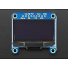
This Flux.ai project is a breakout board for the Adafruit Monochrome 1.3″ 128×64 OLED graphic display (STEMMA QT / Qwiic). It exposes all of the display’s pins on both a standard 0.1″ pitch header and a STEMMA QT / Qwiic connector, plus provides regulated 3.3 V power and level-shifting circuitry so you can easily plug the OLED into any 3.3 V or 5 V microcontroller.
Purpose
- Create a plug-and-play interface for the SSD1306-based OLED module
- Provide both Qwiic/STEMMA QT connectivity and a 1×8, 2.54 mm header
- Include an on-board 3.3 V regulator and level shifters so it works from 5 V or 3.3 V hosts
- Simplify wiring: all control signals, power, and ground are broken out to clearly labeled pins
Core Components
Table
| Component | Role |
|---|---|
| VIN | Raw supply input (e.g., 5 V or 3.3 V from host) |
| 3Vo | On-board 3.3 V regulator output |
| GND | Ground reference |
| RST | Reset line for the OLED driver IC |
| A0/DC | Data/Command select for SSD1306 |
| DATA | SPI MOSI (or I²C SDA if reconfigured) |
| CLK | SPI Clock (or I²C SCL if reconfigured) |
| CS | SPI chip-select line |
| J1 | 1×8 2.54 mm header for all signals and power |
Signal Flow & Interactions
-
Power Section
- [VIN] accepts 5 V (or 3.3 V) from the host.
- On-board LDO/regulator steps this down to 3.3 V on [3Vo].
- [GND] is the common return.
-
Control & Data Lines
- [RST] resets the SSD1306 controller when driven low.
- [A0/DC] tells the display whether incoming bytes are commands (low) or data (high).
- [DATA] and [CLK] carry serial display data via SPI (default) or can be remapped for I²C.
- [CS] enables the SPI interface when low.
-
Breakout Connectors
- [J1] duplicates these pins on a standard 0.1″ header.
- A matching Qwiic/STEMMA QT connector (not shown in schematic yet) provides plug-and-play cabling.
Design & Implementation Steps
-
Schematic Entry
- Place eight terminal symbols for each signal pin.
- Add a 1×8 pin-header footprint (J1) matching both SPI and I²C pinouts.
- Add the 3.3 V regulator (e.g., an SOT-23 LDO) and its necessary input/output decoupling capacitors.
- Insert level-shifter ICs or simple MOSFETs if you need 5 V-to-3.3 V signal translation.
-
Power Regulation
- Route [VIN] → LDO → [3Vo].
- Place a 10 µF and 0.1 µF ceramic cap on both regulator input and output, as close as possible to the device pins.
-
Level Shifting
- If targeting 5 V hosts, add bidirectional MOSFET shifters on [DATA] and [CLK] (and optionally [A0/DC] and [RST]).
- Otherwise, for pure 3.3 V hosts, connect signals directly to the OLED.
-
Connector Footprints
- Include both Qwiic/STEMMA QT (4-pin JST SH) and the 1×8 header for maximum flexibility.
- Silk-screen labels for each pin to avoid confusion.
-
PCB Layout
- Place the regulator and decoupling caps close together for stability.
- Keep traces from [DATA] and [CLK] short to maintain signal integrity up to several MHz.
- Group all power and ground traces with wide pours to minimize voltage drop.
Key Design Choices & Trade-offs
-
On-board Regulation vs. Host-only Power
- On-board LDO adds cost and board area but allows 5 V compatibility.
- Host-only 3.3 V reduces parts but limits you to 3.3 V systems.
-
Level-shifting Method
- MOSFET-based bidirectional shifters support both SPI and I²C on the same pins.
- Resistive dividers are cheaper but only work one-way, may slow edges.
-
Connector Redundancy
- Dual connectors (Qwiic + header) increase flexibility but consume board real estate.
Challenges & Considerations
-
Signal Integrity
- SPI at >10 MHz can suffer ringing; keep traces short and add series damping resistors (~22 Ω).
-
Power Stability
- Ensure low-ESR caps on the regulator; avoid placing other noisy loads on the same rail.
-
Thermal Management
- The LDO will dissipate (VIN–3.3 V)×I; for large currents, consider a switching regulator.
-
EMI/ESD Protection
- For field use, add TVS diodes or series ferrites on exposed lines to protect the OLED.
Real-World Applications
- Wearable displays
- IoT sensor dashboards
- Portable data loggers
- DIY handheld consoles
- Rapid prototyping with Raspberry Pi or Arduino ecosystems
Areas for Improvement & Future Enhancements
-
Switch-Mode Power Supply
- Replace the LDO with a buck converter for efficiency in battery-powered builds.
-
Backlight Adjustment
- Add PWM-controlled brightness via a MOSFET driver.
-
I²C Only Version
- Remove SPI-only pins and optimize footprint for a smaller board.
-
Additional Mounting Options
- Include castellated edges for SMT-mountable versions.
-
Prototyping Pads
- Provide extra breakout pads for logic analyzers or custom signals.
With these building blocks and design guidelines, you have a robust, flexible breakout that can plug directly into almost any development platform, making the 1.3″ SSD1306 display trivially easy to integrate.
Select LDO regulator
Add ESD protection
Calculate LDO dissipation
Placement guidance
Damping resistors
To get started, talk to Flux or create a New Document.

Welcome 👋
Flux accelerates your PCB design with AI.
Create your account to start using this component and bring your ideas to life.