jharwinbarrozo / PTS810SJK250SMTRLFS

Loaded

3

Files

Schematic

PCB

Log InSign Up

Chat

Welcome to Flux

Treat Flux like your intern. Tell it what you'd like to build and it'll get to work. You can also ask it questions, brainstorm ideas, and teach it your preferences. Learn More
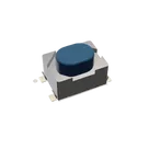
Explain this part
Write a part description
Describe each pin
Operating conditions
Electrical max ratings
Part Specifications
Application circuits
Verify Part Details
Recommend similar parts
Check availability & lifecycle

​
Sign up to send

To get started, talk to Flux or create a New Document.

Reviews

Documents

    Documents are markdown text files which describe project goals, capture details, or even simulation outputs.

    Assets

    kicad_mod

    PTS810SJG250SMTRLFS.kicad_mod

    PTS810SJG250SMTRLFSFootprint
    PTS810SJK250SMTRLFS-thumb.png

    PTS810SJK250SMTRLFS-thumb.png

    PTS810SJK250SMTRLFS-thumbThumbnail
    push-button-open.svg

    push-button-open.svg

    push-button-openDefault
    step

    PTS810SJK250SMTRLFS.step

    3D_PTS810SJK250SMTRLFS3D Model

    PTS810SJK250SMTRLFS

    PTS810SJK250SMTRLFS thumbnail
    PTS 810 Series Microminiature SMT Top Actuated
    Features/Benefits
    • 4.2 x 3.2 mm footprint
    • 2.5 mm thickness
    • High number of cycles
    • Color coded actuators
    Typical Applications
    • Control panels
    • Nomad devices
    • Remote controls
    • Keyless entry system
    3.2mm 2.5mm Round Button 50mA Brick nogging 4.2mm SPST 16V SMD Tactile Switch SPST-NO Top Actuated Surface Mount.

    Properties

    Switch

    PTS810SJK250SMTRLFS

    C&K

    datasheet.lcsc.com/lcsc/1810121650_C-K-PTS810SJK250SMTRLFS_C221896.pdf

    SW

    C221896

    Pricing & Availability

    Distributor

    Qty 1

    Controls

    Welcome 👋

    Flux accelerates your PCB design with AI.

    Create your account to start using this component and bring your ideas to life.

        Introducing AI Placement!
        AI Placement Demo

        AI-Powered Component Placement

        Let AI place your components intelligently. AI Placement analyzes your schematic and positions components for optimal routing, signal integrity, and board density.

        From Schematic to Layout in Seconds

        Skip the tedious manual placement. AI Placement generates a starting layout you can refine, saving hours of repetitive work on every new design.

        Works With Auto-Layout

        Pair AI Placement with Auto-Layout for a complete AI-driven PCB design flow — from component placement through trace routing, all with one click.

        Try it