Chat

Welcome to Flux

Treat Flux like your intern. Tell it what you'd like to build and it'll get to work. You can also ask it questions, brainstorm ideas, and teach it your preferences. Learn More

Explain this part
Write a part description
Describe each pin
Operating conditions
Electrical max ratings
Part Specifications
Application circuits
Verify Part Details
Recommend similar parts
Check availability & lifecycle

explain this project.

@copilot explain this project.
2y
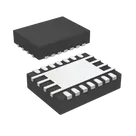
This project revolves around the TPS63020DSJR, which is a Buck-Boost Switching Regulator IC (Integrated Circuit) manufactured by Texas Instruments. Here's an explanation of the major components and terms in your project:
  1. Buck-Boost: This refers to the type of converter the IC employs. A buck-boost converter can step voltage up or step it down, allowing the output voltage to be more or less than the input voltage.
  2. VFDFN Package: IC is packaged in a VFDFN (Very Thin Dual-Flat-No-Leads) format.
  3. Pins: Each designator represents a specific pin of the IC or an external component that interacts with the IC. The pin numbers (from 1 to 15) are referenced in the context of the IC's pin layout.
Key Pin Details:
  • PG (Pin 14) likely stands for "Power Good". It is used as an output to indicate that the output is within the specified voltage level.
  • Both L1 (Pin 8 & 9) and L2 (Pin 6, 7) represent inductors that are used for energy storage in the buck-boost converter.
  • VIN (Pin 10, 11) & VINA (Pin 1) are the input voltage pins, where power is supplied to the IC.
  • VOUT (Pin 4, 5) is the output voltage pin, where power flows out of the IC, typically to other components in the circuit.
  • GND (Pin 2) is the ground reference point.
  • EPAD (Pin 15) is the exposed pad, which is typically soldered to a ground plane for thermal relief.
  • PS/SYNC (Pin 11) is used to set the switching frequency of the regulator.
  • FB (Pin 3) stands for "Feedback" and it's used for voltage regulation by making a comparison with the reference voltage.
  • EN (Pin 12) stands for "Enable". The IC starts to function when this pin is pulled high.
Please note that:
  • No electrical connections have been made in this project yet. It's a blank schematic awaiting the user to connect the components as per the application requirements.
  • Some of the pins like VINA, VIN, and VOUT appear to be duplicated, which might be an error in the documentation or it might be intentional, depending on the design needs.
Lastly, the project license is ambigious as well, with it referencing Creative Commons License URL, but no specific license type mentioned.
This is an overall explanation, aimed to give a quick overview, not a deep technical analysis. Let me know whether you'd like further explanation on any area. It's also important to consult the datasheet of the TPS63020DSJR for a complete understanding its functionality and pin descriptions.
2y
Someone is typing...
3

No files yet

Documents

    Documents are markdown text files which describe project goals, capture details, or even simulation outputs.

    Assets

    TPS63020_DSJ_14

    TPS63020_DSJ_14

    defaultDefault
    TPS63020DSJR.png

    TPS63020DSJR.png

    TPS63020DSJRThumbnail
    kicad_mod

    TPS63020DSJR.kicad_mod

    Footprint_V5Footprint
    stp

    DSJ0014A.stp

    3D3D Model

    TPS63020DSJR

    TPS63020DSJR thumbnail
    Buck-Boost Switching Regulator IC Positive Adjustable 1.2V 1 Output 3.5A (Switch) 14-VFDFN Exposed Pad #CommonPartLibrary #IntegratedCircuit #PowerManagement #VoltageRegulator #BuckBoost #Regulator

    Properties

    Integrated Circuit

    Texas Instruments

    TPS63020DSJR

    U

    Pricing & Availability

    Distributor

    Qty 1

    Controls