Chat
Welcome to Flux
Treat Flux like your intern. Tell it what you'd like to build and it'll get to work. You can also ask it questions, brainstorm ideas, and teach it your preferences. Learn More
Explain this part
Write a part description
Describe each pin
Operating conditions
Electrical max ratings
Part Specifications
Application circuits
Verify Part Details
Recommend similar parts
Check availability & lifecycle

himeth
Image
copilot
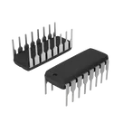
- Dual JK Flip-Flop with Clear and Preset
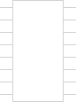
- Pinout:
- 1: Clear (CLR1)
- 2: Preset (PRE1)
- 3: Clock (CLK1)
- 4: J (J1)
- 5: K (K1)
- 6, 7: Q and Q' (Q1, Q1')
- 8: GND
- 9, 10: Q and Q' (Q2, Q2')
- 11: K (K2)
- 12: J (J2)
- 13: Clock (CLK2)
- 14: Preset (PRE2)
- 15: CLR (CLR2)
- 16: VCC
Example Connection for Two JK Flip-Flops-
First JK Flip-Flop (U1A)
- Connect Clock: Connect external clock signal to $U1:3$.
- Connect Preset: Connect $U1:2$ to VCC.
- Connect Clear: Connect $U1:1$ to GND.
- Connect Inputs: Connect initial input to $U1:4$ and $U1:5$.
- Connect Outputs:
- $U1:6$ (
- $U1:7$ to a ground plane if unused.
-
Second JK Flip-Flop (U1B)
- Connect Clock: Connect $U1:13$ to $U1:6$.
- Connect Preset: Connect $U1:14$ to VCC.
- Connect Clear: Connect $U1:15$ to GND.
- Connect Inputs: Connect $U1:12$ and $U1:11$ to VCC (or depending on the desired functionality).
- Connect Outputs:
- $U1:9$ (
- $U1:10$ to GND if not used.
Configuration for Second Flip Flop (U2)Q1) to $R1$ and next JK flip-flop input.Q2) to $R2$ and next JK flip-flop input.-
First JK Flip-Flop (U2A)
- Connect Clock: Connect $U2:3$ to $U1:9$ (
- Connect Preset: Connect $U2:2$ to VCC.
- Connect Clear: Connect $U2:1$ to GND.
- Connect Inputs: Connect $U2:4$ and $U2:5$ to VCC.
- Connect Outputs:
- $U2:6$ (
- $U2:7$ to a ground plane if unused.
-
Second JK Flip-Flop (U2B)
- Connect Clock: Connect $U2:13$ to $U2:6$.
- Connect Preset: Connect $U2:14$ to VCC.
- **Connect Clear: **Connect $U2:15$ to GND.
- Connect Inputs: Connect $U2:12$ and $U2:11$ to VCC.
- Connect Outputs:
- $U2:9$ (
- $U2:10$ to GND if unused.
Connections SummaryQ2).Q1) to $R3$ and next JK flip-flop input.Q2) to $R4$ and next JK flip-flop input.himeth
copilot
- Initial voltage (V1): 0V
- Peak voltage (V2): 1V
- Time delays (TD): 2n
- Rise time (TR): 2n
- Fall time (TF): 2n
- Pulse width (PW): 50n
- Period (PER): 100n
SPICE Netlist Example:Image
Image
Image