Chat

Welcome to Flux

Treat Flux like your intern. Tell it what you'd like to build and it'll get to work. You can also ask it questions, brainstorm ideas, and teach it your preferences. Learn More

Explain this part
Write a part description
Describe each pin
Operating conditions
Electrical max ratings
Part Specifications
Application circuits
Verify Part Details
Recommend similar parts
Check availability & lifecycle
Step-by-Step Instructions: Connect Power and Ground: Connect Pin 14 (Vcc) of th...

@copilot Step-by-Step Instructions: Connect Power and Ground:
Connect Pin 14 (Vcc) of the 74HC74 to the positive terminal of your power supply (5V). Connect Pin 7 (GND) of the 74HC74 to the ground. Connect the RC Circuit to Generate Clock Pulse:
Connect a 10 kΩ resistor (R1) between the power supply (+5V) and the clock input (Pin 3) of the 74HC74. Connect a 10 µF capacitor (C1) between the clock input (Pin 3) and ground. Configure the Flip-Flop for Toggling:
Connect the Q' output (Pin 6) of the 74HC74 to the D input (Pin 2). This configuration will ensure that the flip-flop toggles its state with every clock pulse. Leave the Set (Pin 4) and Reset (Pin 1) inputs unconnected or connect them to the ground if you want the flip-flop to operate normally without forced resets. Connect the Output:
The toggled output can be taken from the Q output (Pin 5). This will be the output that changes state every time the power is cycled.
1y
It looks like you have a good step-by-step plan to set up the 74HC74 flip-flop. However, our current project is using the SN74HC374N, which is an 8-bit D-type flip-flop.
Nonetheless, I can provide a similar connection plan with the correct pin numbers for the SN74HC374N:
Step-by-Step Instructions: 1. Connect Power and Ground:
  • Connect the power supply to the Vcc and GND pins of the SN74HC374N.
    • Connect VCC:Pin 20\text{VCC}:\text{Pin 20} to the positive terminal of the power supply (5V).
    • Connect GND:Pin 10\text{GND}:\text{Pin 10} to ground.
2. Connect the RC Circuit to Generate Clock Pulse:
  • Let's assume we use additional resistors and capacitors named R1 and C1.
    • Connect a 10 kΩ resistor (R1) between the power supply (+5V) and the clock input.
    • Connect R1:1\text{R1:1} to Vcc (5V).
    • Connect the other end of R1 to CLK:Pin 11\text{CLK}:\text{Pin 11}.
    • Connect a 10 µF capacitor (C1) between the clock input and ground.
    • Connect one end of C1 to CLK:Pin 11\text{CLK}:\text{Pin 11}.
    • Connect the other end of C1 to ground.
3. Configure the Flip-Flop for Toggling:
  • Connect the Q' output of the flip-flop to the D input to configure toggling on each clock pulse.
    • Connect Q1:Pin 2\text{Q1}:\text{Pin 2} to D1:Pin 3\text{D1}:\text{Pin 3}.
    • Connect Q2:Pin 5\text{Q2}:\text{Pin 5} to D2:Pin 4\text{D2}:\text{Pin 4}.
    • Continue similarly for the remaining Q to D connections.
  • For normal operation without resets:
    • Connect OE:Pin 1\text{OE}:\text{Pin 1} to ground.
4. Connect the Output:
  • Take the toggled output from the Q output. For example:
    • The toggled output can be taken from Q8:Pin 19\text{Q8}:\text{Pin 19}, which will change state with each clock pulse.
In summary, here are the explicit connections:
  • Connect VCC:Pin 20 to the positive terminal of the power supply (5V).
  • Connect GND:Pin 10 to ground.
  • Connect R1:1 to VCC:Pin 20.
  • Connect R1:2 to CLK:Pin 11.
  • Connect C1:1 to CLK:Pin 11.
  • Connect C1:2 to ground.
  • Connect Q1:Pin 2 to D1:Pin 3.
  • Connect Q2:Pin 5 to D2:Pin 4.
  • Continue similarly for the remaining Q to D connections (with exact designators).
Would you like to proceed with any other specific steps or validations?
1y
yes proced
1y
Great! Let's break down the connections step-by-step for the SN74HC374N. I'll provide a schematic based on your requirements:
Step-by-Step Connection Instructions: 1. Connect Power and Ground:
  • Connect Vcc:
    • Connect VCC:Pin 20 to the positive terminal of your power supply (5V).
    • ConnectGND:Pin 10toground.\text{Connect} \, \text{GND:Pin 10} \, \text{to} \, \text{ground.}
2. Connect the RC Circuit to Generate Clock Pulse:
  • Resistor (R1):
    • Connect one end of a 10 kΩ resistor (R1) to the positive terminal of the power supply (5V).
    • Connect the other end of R1 to CLK:Pin 11\text{CLK:Pin 11} (Clock pin).
  • Capacitor (C1):
    • Connect one end of a 10 µF capacitor (C1) to CLK:Pin 11\text{CLK:Pin 11}.
    • Connect the other end of C1 to ground. Connect C1:2 to GND (Ground).
3. Configure the Flip-Flop for Toggling:
  • Connect each Q output to the corresponding D input in a loop to enable toggling:
    • Connect 1Q:Pin 2 to 1D:Pin 3.
    • Connect 2Q:Pin 5 to 2D:Pin 4.
    • Connect 3Q:Pin 6 to 3D:Pin 7.
    • Connect 4Q:Pin 9 to 4D:Pin 8.
    • Connect 5Q:Pin 12 to 5D:Pin 13.
    • Connect 6Q:Pin 15 to 6D:Pin 14.
    • Connect 7Q:Pin 16 to 7D:Pin 17.
    • Connect 8Q:Pin 19 to 8D:Pin 18.
4. Connect the Output:
  • Take the toggled output from any Q output. Example:
    • Toggle output can be taken from 8Q:Pin 19.
Here's a summary of the connections with more precise references:
  • Power and Ground:
    • Connect VCC:Pin 20 to the positive terminal of the power supply (5V).
    • Connect GND:Pin 10 to ground.
  • RC Circuit (Clock Pulse):
    • Connect R1:1 to Vcc (5V).
    • Connect R1:2 to CLK:Pin 11\text{CLK:Pin 11}.
    • Connect C1:1 to CLK:Pin 11\text{CLK:Pin 11}.
    • Connect C1:2 to GND.
  • Flip-Flop Configuration:
    • Connect 1Q:2 to 1D:3.
    • Connect 2Q:5 to 2D:4.
    • Connect 3Q:6 to 3D:7.
    • Connect 4Q:9 to 4D:8.
    • Connect 5Q:12 to 5D:13.
    • Connect 6Q:15 to 6D:14.
    • Connect 7Q:16 to 7D:17.
    • Connect 8Q:19 to 8D:18.
Is this the setup you had in mind? Or do you need any adjustments or additional configurations?
1y
Someone is typing...
2
5Q
3Q
4D
6Q
3D
2D
8Q
VCC
6D
7Q
CLK
8D
7D
5D
1Q
1D
GND
2Q
4Q
OE

No files yet

Documents

    Documents are markdown text files which describe project goals, capture details, or even simulation outputs.

    Assets

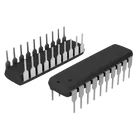
    DIP-20_W7.62mm-3D.step

    DIP-20_W7.62mm-3D.step

    DIP-20_W7.62mm-3D3D Model
    DIP-20_W7.62mm-removebg-preview.png

    DIP-20_W7.62mm-removebg-preview.png

    DIP-20_W7.62mm-removebg-previewThumbnail
    svg

    20Pins

    defaultDefault
    kicad_mod

    DIP-20_W7.62mm-Footprint_S.kicad_mod

    DIP-20_W7.62mm-Footprint_SFootprint

    SN74HC374N

    SN74HC374N thumbnail
    Flip Flop 1 Element D-Type 8 Bit Positive Edge 20-DIP (0.300", 7.62mm) #CommonPartsLibrary #IntegratedCircuit #Logic #Flip-Flops #74HC374

    Properties

    Integrated Circuit

    Texas Instruments

    SN74HC374N

    U

    Pricing & Availability

    DPN

    Stock

    Qty 1

    5

    0–1.1K

    $0.7294–$1.048

    1

    0

    $0.00

    1

    265

    $0.92503

    1

    10

    $0.832

    1

    2K

    $1.72

    1

    1K

    $1.69

    3

    270–1.1K

    $1.0334–$1.048

    Controls