Schematic Component Review
Thought for 6 mins 10 sec
Here’s a compact in-line car-audio bass level controller with an integrated voltmeter and remote turn-on control, optimized for low-noise passive audio and robust 12 V automotive power.
Block diagram
Diagram
Recommended components from the library
Audio path
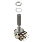
- Dual-gang 50k audio taper potentiometer:
- PDB182-K430K-503A (Bourns, 50k log, dual gang). Note: verify/choose the variant with integrated SPST “click” switch for the remote control requirement; if not available, pick the switch-equipped version in the PDB18 family.
- RCA jacks (4x, female, board mount):
Power input and protection
- Power headers:
- B2B-XH-A(LF)(SN) (JST-XH 2-pin, +12V/GND)
- B3B-XH-A(LF)(SN) (JST-XH 3-pin, REM_IN/REM_OUT/GND)
- TVS diode (58 V class for automotive transients; pick one of):
- SMBJ58A-13-F or
- SMBJ58A-QH or
- SMAJ58A-TR
- Reverse-polarity protection:
- Series Schottky SS34, or ideal-diode PFET topology
- Input EMI filtering:
- Ferrite bead BLM21PG121SN1D (place on +12V after fuse)
- 5 V regulator (for MCU/display):
- LM2940S-5.0 (automotive-friendly LDO)
- Input protection fuse:
- 0805L110WR (PTC resettable)
Remote turn-on switching
- High-side PFET (12 V signal line):
- AO3407A (SOT-23 P-MOSFET)
Controller and display
- MCU (compact, with ADC):
- 4-digit LED display (simplest BOM as a module):
- TM1637 4-digit module (horizontal)
- If you prefer discrete IC + LED, use driver TM1637 plus a suitable 4-digit 7-seg display.
Voltage sensing and decoupling passives
- ADC divider (typical values; confirm for your ADC range and impedance):
- Upper: RMCF0603FG100K
- Lower: CRCW060333K0JNEAC
- Bypass caps:
Design notes (applied best practices)
- Grounding for low noise: prioritize ground separation (audio return vs. digital/display return) because return paths dominate noise coupling. Tie at a single star near the power entry or RCA ground reference.
- ADC divider drive: check divider output impedance using (R1*R2)/(R1+R2). If it exceeds the MCU ADC input spec, buffer or lower the divider values.
- Regulator sizing: ensure the 5 V regulator supports total load current with a 25% buffer, and operate power ICs at no more than 75% of their rated maximum power.
- Supply bypassing: switching/display noise issues are often fixed by proper bypassing first; place 100 nF at each IC VCC pin and keep traces short.
- Audio THD: keep the audio path passive (dual 50k log pot between RCA IN/OUT), route audio away from the digital display and 12 V rails, and use a star ground at the RCA shield.
Clarify before we implement
- Potentiometer with switch: OK to use the Bourns PDB18 family and select the variant with integrated SPST “click” switch? If you prefer Alpha/WH148 style, I can swap to that family.
- Display choice: keep the TM1637 module for speed, or switch to a discrete LED + driver for a slimmer board?
- Headers: confirm pin order for JST-XH 3-pin remote header (e.g., 1=REM_IN, 2=GND, 3=REM_OUT).
Confirm pot with switch
Choose display style
Ask for divider calculation
Grounding/layout guidance
Remote header pinout