i.MX6 Proje Arayışı
2:22
Parsing project intents.
Issuing knowledge queries.
Defining PMIC candidates.
Considering PMIC and connector options.
Choosing components for the plan.
Accessing knowledge base.
Preparing execution plan.
- MCIMX6D5EYM10AD, 24 MHz/RTC kristaller, düşük maliyet PMIC (güç IC’lerini tam yüklerinin en fazla %75’iyle seçeceğim), 2 GB için 32‑bit DDR3L (4×8Gb x16, 2 rank), eMMC 16GB ve iki adet 0.5 mm, ~100 pin SOM konnektörü eklenecek.
- Design an i.MX6D Dual SOM incorporating the MCIMX6D5EYM10AD SoC, 2 GB of DDR3L memory, and 16 GB eMMC storage. The design should prioritize low cost and high availability, follow datasheet guidelines and proven open-source references, and include PMIC selection and SOM connectors (which will later be finalized by the user).
-
SoC, Clocks, and Power
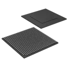
- Add the MCIMX6D5EYM10AD symbol to the schematic.
- Add a 24 MHz main crystal oscillator and the RTC crystal.
- Select a cost-effective PMIC (using a low cost, high availability default from the library) and add it to the schematic. Dimension the power rails and add decoupling capacitors, ensuring that no power IC is used beyond 75% of its rated power.
-
DDR3L Memory Integration
- Add DDR3L components to achieve 2 GB capacity using a 32-bit bus configuration with four 8 Gb x16 devices arranged in two ranks.
- Include required VREF circuitry, terminations, and decoupling components.
- Apply length and impedance matching guidelines per the i.MX6 DDR design recommendations.
-
eMMC Storage Integration
- Add a 16 GB eMMC component that complies with JEDEC 5.x standards.
- Connect the eMMC to a USDHC port with proper pull-ups, series options, and decoupling capacitors.
- Enforce proper clock routing constraints as per datasheet specifications.
-
Boot, Reset, and Debug Design
- Implement boot strap resistors ensuring eMMC-first boot setup.
- Add a POR supervisor, ONOFF/POR_B circuitry and configure reset signals.
- Expose UART and JTAG headers for debug purposes.
-
Carrier Connectors
- Add two low-cost, widely available 0.5 mm pitch board-to-board connectors (approximately 2 x 100 pins) from the library.
- Map key interfaces such as USDHC, RGMII, USB, I2C, SPI, GPIO, and power through these connectors.
-
Review and Finalization
- Run ERC and DRC checks to ensure design correctness.
- Review parts availability and include notes for layout rules including DDR impedance management and keep-out areas.
- Update the project description and metadata to reflect these changes.
- The schematic includes the i.MX6D SoC, DDR3L memory, and eMMC components with proper connections and power regulation.
- Power subsystems and decoupling meet the derating guidelines (not exceeding 75% load on power ICs).
- Boot, reset, and debug circuitry is correctly implemented and mapped to user accessible interfaces.
- Carrier connectors are present and key interfaces are correctly routed for future board-to-board connection.
Started implementing a plan
# Goal
- Design an i.MX6D Dual SOM incorporating the MCIMX6D5EYM10AD SoC, 2 GB of DDR3L memory, and 16 GB eMMC storage. The design should prioritize low cost and high availability, follow datasheet guidelines and proven open-source references, and include PMIC selection and SOM connectors (which will later be finalized by the user).
# Implementation plan
1. SoC, Clocks, and Power
1. Add the MCIMX6D5EYM10AD symbol to the schematic.
2. Add a 24 MHz main crystal oscillator and the RTC crystal.
3. Select a cost-effective PMIC (using a low cost, high availability default from the library) and add it to the schematic. Dimension the power rails and add decoupling capacitors, ensuring that no power IC is used beyond 75% of its rated power.
2. DDR3L Memory Integration
1. Add DDR3L components to achieve 2 GB capacity using a 32-bit bus configuration with four 8 Gb x16 devices arranged in two ranks.
2. Include required VREF circuitry, terminations, and decoupling components.
3. Apply length and impedance matching guidelines per the i.MX6 DDR design recommendations.
3. eMMC Storage Integration
1. Add a 16 GB eMMC component that complies with JEDEC 5.x standards.
2. Connect the eMMC to a USDHC port with proper pull-ups, series options, and decoupling capacitors.
3. Enforce proper clock routing constraints as per datasheet specifications.
4. Boot, Reset, and Debug Design
1. Implement boot strap resistors ensuring eMMC-first boot setup.
2. Add a POR supervisor, ONOFF/POR_B circuitry and configure reset signals.
3. Expose UART and JTAG headers for debug purposes.
5. Carrier Connectors
1. Add two low-cost, widely available 0.5 mm pitch board-to-board connectors (approximately 2 x 100 pins) from the library.
2. Map key interfaces such as USDHC, RGMII, USB, I2C, SPI, GPIO, and power through these connectors.
6. Review and Finalization
1. Run ERC and DRC checks to ensure design correctness.
2. Review parts availability and include notes for layout rules including DDR impedance management and keep-out areas.
3. Update the project description and metadata to reflect these changes.
# Success criteria
- The schematic includes the i.MX6D SoC, DDR3L memory, and eMMC components with proper connections and power regulation.
- Power subsystems and decoupling meet the derating guidelines (not exceeding 75% load on power ICs).
- Boot, reset, and debug circuitry is correctly implemented and mapped to user accessible interfaces.
- Carrier connectors are present and key interfaces are correctly routed for future board-to-board connection.
Working...
To get started, talk to Flux or create a New Document.

Welcome 👋
Flux helps you build PCBs faster with an AI teammate!
Create your account to collaborate, stay updated, fork your own version, and get instant answers from our AI agent.