ESP32-C3-MINI Pin Analysis

Check datasheet for this component and make lists of bootstrap pins, input only pins, pins connected to internal memory, USB pins(if present)
Worked for 1 min 28 sec
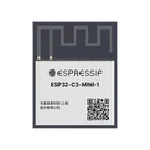
I extracted the ESP32-C3-MINI-1-N4 datasheet pin groups into a project file: ESP32-C3-MINI-1-N4 special pin lists from datasheet. Summary: strapping/bootstrap pins are IO2/GPIO2, IO8/GPIO8, IO9/GPIO9; the only input-only pin is EN; USB pins are IO18/USB_D− and IO19/USB_D+; internal flash uses chip-side SPI0/1 signals GPIO12–GPIO17, not exposed as module pins.
Check special pins
Review 3V3 rail
Document pin constraints
Inspect USB nets
Refine this doc
Ask about this doc
ESP32-C3-MINI-1-N4 special pin lists from datasheet
Source: Espressif ESP32-C3-MINI-1 & ESP32-C3-MINI-1U Datasheet v2.1, project Datasheet URL.
Bootstrap / strapping pins
The datasheet calls these strapping pins:
Table
| Module pin name | Module pin no. | GPIO | Default configuration | Boot/config role |
|---|---|---|---|---|
| IO2 | 5 | GPIO2 | Floating | Chip boot mode; recommended pulled up due to glitches |
| IO8 | 22 | GPIO8 | Floating | Chip boot mode; ROM message printing control |
| IO9 | 23 | GPIO9 | Weak pull-up, bit value 1 | Chip boot mode |
Boot-mode table from datasheet:
Table
| Boot mode | GPIO2 | GPIO8 | GPIO9 |
|---|---|---|---|
| SPI boot mode | 1 | Any value | 1 |
| Joint download boot mode | 1 | 1 | 0 |
Notes from datasheet: strapping pins are sampled at chip reset; hold time after CHIP_EN high is 3 ms. After reset, the pins are freed for regular IO use.
Input-only pins
The only module pin listed as type I is:
Table
| Module pin name | Module pin no. | Type | Function |
|---|---|---|---|
| EN | 8 | I | High enables the chip; low powers it off. Datasheet note: do not leave EN floating. |
All exposed GPIO pins in the module pin table are listed as I/O/T, not input-only.
Pins connected to internal / in-package flash memory
For the module-level exposed pins, the datasheet does not list GPIO12–GPIO17 as exposed module pins. It states SPI0/SPI1 are used to access in-package or off-package flash, and SPI0/1 pins are multiplexed with GPIO12–GPIO17 via IO MUX. In the module schematic, these chip flash pins are connected internally to the in-package SPI flash and are not broken out as module pins.
Internal flash-related chip signals shown in the module schematic:
Table
| Chip signal | Related GPIO / function | Notes |
|---|---|---|
| SPIHD | GPIO12 | Internal flash SPI signal |
| SPIWP | GPIO13 | Internal flash SPI signal |
| SPICS0 | GPIO14 | Internal flash chip-select signal |
| SPICLK | GPIO15 | Internal flash clock signal |
| SPID | GPIO16 | Internal flash data signal |
| SPIQ | GPIO17 | Internal flash data signal |
Important distinction: some exposed module pins have FSPI alternate functions for general-purpose SPI2 / IO MUX usage, but those are not the internal in-package flash pins:
Table
| Exposed module pin | Module pin no. | Alternate FSPI function listed |
|---|---|---|
| IO2 | 5 | FSPIQ |
| IO10 | 16 | FSPICS0 |
| IO4 | 18 | FSPIHD |
| IO5 | 19 | FSPIWP |
| IO6 | 20 | FSPICLK |
| IO7 | 21 | FSPID |
USB pins
The module includes USB Serial/JTAG support. The datasheet states USB_D+ and USB_D− are multiplexed with GPIO19 and GPIO18.
Table
| Module pin name | Module pin no. | USB function | GPIO |
|---|---|---|---|
| IO18 | 26 | USB_D− | GPIO18 |
| IO19 | 27 | USB_D+ | GPIO19 |
USB Serial/JTAG features listed include USB 2.0 full-speed device, CDC-ACM, JTAG debugging, and firmware flashing. The queried datasheet text also notes USB 2.0 full-speed up to 12 Mbit/s and no 480 Mbit/s high-speed mode.
Bootstrap / strapping pins
Input-only pins
Pins connected to internal / in-package flash memory
USB pins