Chat

Welcome to Flux

Treat Flux like your intern. Tell it what you'd like to build and it'll get to work. You can also ask it questions, brainstorm ideas, and teach it your preferences. Learn More

Explain this part
Write a part description
Describe each pin
Operating conditions
Electrical max ratings
Part Specifications
Application circuits
Verify Part Details
Recommend similar parts
Check availability & lifecycle
please explain what VCC, C, CHANNELS\_IN/OUT6, CHANNEL\_IN/OUT0, CHANNEL\_IN/OUT...

@copilot please explain what VCC, C, CHANNELS_IN/OUT6, CHANNEL_IN/OUT0, CHANNEL_IN/OUT3, COMOUT/IN, CHANNEL_IN/OUT2, INH, CHANNEL_IN/OUT7, VSS, B, CHANNELS_IN/OUT4, CHANNEL_IN/OUT1, VEE, A, CHANNEL_IN/OUT5 do.
2y
In a CD4051BE multiplexer/demultiplexer IC, the pin functions are critical for understanding how to design and implement circuits using this chip. Let's describe the roles of each pin based on your project's designators:
  1. VCC (Pin 16): This is the positive power supply voltage pin. It supplies power to the IC for its operation.
  2. C (Pin 9): Generally, the designation "C" might be referring to a control or configuration pin in some contexts, but for the CD4051BE, Pin 9 is actually the common output/input (COM) in demultiplexing/multiplexing configurations.
  3. CHANNELS_IN/OUT6 (Pin 2), CHANNEL_IN/OUT0 (Pin 13), CHANNEL_IN/OUT3 (Pin 12), CHANNEL_IN/OUT2 (Pin 15), CHANNEL_IN/OUT7 (Pin 4), CHANNELS_IN/OUT4 (Pin 1), CHANNEL_IN/OUT1 (Pin 14), CHANNEL_IN/OUT5 (Pin 5): These pins are the data input/output channels. In a multiplexer configuration, one of these channels is connected to the common port (COM) based on the binary code applied to the selection inputs. In a demultiplexer configuration, the signal at the common port is routed to one of these outputs based on the selection input.
  4. COMOUT/IN (Pin 3): This serves as the common port for input in the case of multiplexing and output in the case of demultiplexing.
  5. INH (Pin 6): This is the inhibit pin. When high, it disables all channels from connecting to the common port, effectively disconnecting the common port from all channels.
  6. VSS (Pin 8): This is the ground or negative supply voltage pin. It's connected to the ground of your circuit.
  7. B (Pin 10), A (Pin 11): These pins, along with another selection pin not explicitly listed here but typically referred to as "S" or "C" (not to be confused with your usage of "C" for pin 9), form the selection inputs that determine which channel is connected to the common port. These are binary inputs that provide a three-bit binary code in multiplexer and demultiplexer applications.
  8. VEE (Pin 7): This is the negative voltage supply pin. In some applications, this pin can be used to supply a negative voltage if needed by the IC for its operation.
Each of these pin functions is crucial for the operation of the CD4051BE as a multiplexer or demultiplexer. By applying signals and voltage levels to these pins accordingly, you can control the routing of signals through the IC for your specific application needs.
2y
Someone is typing...
2
list all VCC pins in a table format. For each pin provide its pin number, pin na...

@copilot list all VCC pins in a table format. For each pin provide its pin number, pin name and function.
1y
Certainly! Based on the provided project and the datasheet, I can extract and format the details for the Vcc pins. Here's a table summarizing that information:

Table


Pin NumberPin NameFunction
16VCCSupply voltage terminal
These details include the pin number, pin name, and function for the Vcc pin on the CD4051BE. If you need more details or information about other pins, feel free to ask.
1y
Someone is typing...
3
VCC
C
CHANNELS_IN/OUT6
CHANNEL_IN/OUT0
CHANNEL_IN/OUT3
COMOUT/IN
CHANNEL_IN/OUT2
INH
CHANNEL_IN/OUT7
VSS
B
CHANNELS_IN/OUT4
CHANNEL_IN/OUT1
VEE
A
CHANNEL_IN/OUT5

To get started, talk to Flux or create a New Document.

Documents

    Documents are markdown text files which describe project goals, capture details, or even simulation outputs.

    Assets

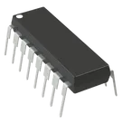
    DIP-16_W7.62mm-removebg-preview.png

    DIP-16_W7.62mm-removebg-preview.png

    DIP-16_W7.62mm-removebg-previewThumbnail
    kicad_mod

    CD4051BE.kicad_mod

    FP_CD4051BEFootprint
    16Pins

    16Pins

    defaultDefault
    stp

    N0016A.stp

    3D_N0016A3D Model

    CD4051BE

    CD4051BE thumbnail

    Properties

    Integrated Circuit

    Texas Instruments

    CD4051BE

    U

    Pricing & Availability

    Distributor

    Qty 1

    Controls