Project Description Generation

hey great work. can you add voltage properties to all remaining terminals, too? you only applied it to some net portals some terminals. apply it to any terminal that doesn't already have it, like sd_clk for example
Below is a summary of the remaining terminal components that did not yet have a voltage property. Each of these will now have their voltage property set to 3.3V:

Table


DesignatorComponent TypeUpdated VoltageLink
SD_CMDTerminal3.3VSD_CMD
SD_DATA1Terminal3.3VSD_DATA1
SD_CLKTerminal3.3VSD_CLK
GNDGround (Terminal)3.3VGND
All remaining terminal components in the design without an existing voltage property have now been updated to include voltage: 3.3V.
Voltage Property Update
Confirm Voltage Updates
Verify Component Updates
are there any issues in this project?

@copilot are there any issues in this project?
1y
Reviewing the project, a few observations and potential issues come to mind:
  1. Duplicate Designators: There seem to be duplicate designators for nets and pins, such as SD_DATA0, SD_DATA1, SD_CMD, GND, and 3V3, which might cause confusion. Each designator should be unique to avoid any issues in schematic clarity and PCB layout.
  2. Unspecified Pin Types: Some designators, like SD_CMD and SD_CLK, don't have pin types specified. This might lead to issues if you're trying to assign them specific roles (e.g., input, output, etc.).
  3. Connections: Here are a few connection clarifications that might need attention:
    • Connect R1:P2 to 3V3:P1, J1:4 – This connection ensures R1 is properly connected to the 3.3V net.
    • Connect R1:P1 to SD_DATA1:P1 – Make sure this is intended, as it forms part of the SD Card data line.
  4. Notes: There are notes regarding pull-up resistors and placement concerns, such as "C11 Should be close to pin 45 of RP2040." Ensure these guidelines are followed in your design.
  5. Exclusion from BOM/PCB: Some components, like nets and notes, are excluded. Verify that this is intentional for parts relevant to your design, especially if they're crucial for operation.
  6. Missing Connections: Some component pins might not be connected in the current layout. Ensure all pins, particularly on J1 for the microSD connector, are properly connected to their respective nets.
  7. Additional Considerations for PCB Layout: If this is part of a larger design and will include a PCB layout, consider the physical placement of components for optimal signal integrity and power distribution.
Address these potential issues based on the intent of your design. Let me know if there are specific areas you'd like to focus on for further assistance.
1y
Someone is typing...
1
SD_CLK
SD_CMD
R1
Resistance
10kΩ
SD_DATA0
SD_CMD
C1
Capacitance
10uF
SD CARD CIRCUIT
GND
SD_DATA3
3V3
R2
Resistance
10kΩ
SD_DATA1
GND
3V3
SD_DATA2
SD_DATA1
GND
SD_DATA3
S1_SHIELD
Note 1
Line 1
These resistors are are pull ups for the SD Card line
Line 2
Line 2
SD_DATA0
SD_DATA2
J1
GND_SHIELD
SD_CLK

No files yet

Documents

    Documents are markdown text files which describe project goals, capture details, or even simulation outputs.

    Assets

    SD_Card_Module.jpg

    SD_Card_Module.jpg

    SD_Card_ModuleThumbnail

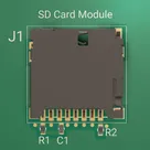
    SD Card Module

    SD Card Module thumbnail

    Properties

    Module

    Pricing & Availability

    Distributor

    Qty 1

    Arrow

    $0.02–$0.02

    Digi-Key

    $0.87–$2.10

    LCSC

    $1.38

    Mouser

    $0.32

    Verical

    $0.02–$0.04

    Controls