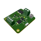
Schematic Design Analysis
1:50
Below is a schematic-level analysis based solely on the provided design information:
1. Regulator & Feedback Network Connections
-
Issue: U3 (SY6280) Pin Misassignment
– Observation: The net labeled VIN shows that both the VIN and EN pins of U3 are tied together. For the SY6280 (pins: VOUT, GND, ISET, EN, VIN), the EN pin should be driven (typically via a pull‐up or by logic) rather than being hardwired with the input voltage.
– Recommendation: Separate U3’s EN from its VIN. Tie EN to the proper logic (or use a resistor divider/pull‑up if that is the intent) per the datasheet recommendation. -
Issue: Shared Divider Resistor (R3) Across Different Nets
– Observation: Resistor R3 has one terminal on net FB (used for U1’s feedback) and the other on net VIN (which also carries U3 VIN/EN). This forces an unexpected connection between two regulator sections that should be independent.
– Recommendation: Redefine the feedback divider so that each regulator (U1 and U3) has its own, isolated divider network. In particular, re‑assign R3’s connections so that the divider for U1’s FB is not shorted to U3’s power section. -
Issue: Conflicting Voltage Divider Formulas
– Observation: The text note “SETTING OUTPUT VOLTAGE” shows two formulas:
This suggests either a design revision or a leftover note from an earlier revision.
– Recommendation: Decide on one feedback network configuration. Remove or update the annotation to reflect the chosen resistor divider between the correct regulator output and its FB pin.
2. Power Distribution & Net Labeling
-
Issue: Duplicate and Ambiguous Net Labels
– Observation: Several portals use similar or duplicate names (for example, multiple “Ground” objects, “12_5V” vs. “12V_DIV” nets) and some nets appear in more than one context (e.g. “VIN” carries U3 VIN and also ties in divider elements for U1).
– Recommendation:- Ensure that each power rail (battery, solar, USB, regulated outputs) is clearly defined with a unique net name.
- Verify that regulator inputs, outputs, and feedback networks use separate nets unless intentional.
- Use consistent naming (for example, avoid “12_5V” and “12V_DIV” if they refer to the same rail or divider) so that the intended connectivity is unambiguous during layout and DRC checks.
-
Issue: Potential Overlap of Regulator Sections
– Observation: The sharing of net VIN between U3 (a SY6280 regulator) and the feedback divider of U1 (RT8059) suggests that their power paths might interfere.
– Recommendation: Completely separate the power and control nets for each converter so that no accidental bridging (for instance, tying U3’s EN/VIN with U1’s divider) occurs.
3. Decoupling Capacitors & Bypass Networks
- Issue: Decoupling Capacitor Placement Uncertainty
– Observation: Although several capacitors (e.g. C1, C2, C8, C9) are present on the schematic, their placement relative to the regulator ICs is not explicitly shown. Given the high switching frequency of devices like the MT3608 and likely for the RT8059, nearby bypass/external output capacitors are critical.
– Recommendation:- Confirm that each regulator has at least one decoupling capacitor placed as close as possible to its VIN, VOUT, and FB pins (if recommended), following datasheet recommendations.
- If not already done, move the decoupling capacitors (for example, C2 for U3’s VIN and C8 for the FB divider) to minimize parasitic inductance.
4. Current Limiting & LED Drive
- Issue: LED Current Limiting
– Observation: The schematic includes two LED components (D5 and D2) with forward voltages and current ratings given, but there is no series resistor explicitly associated with them. Directly connecting an LED to a power rail without a current‐limiting resistor can cause overcurrent damage.
– Recommendation:- Insert an appropriate current-limiting resistor in series with each LED. For example, for a red LED with a forward voltage around 2.0 V and a target current of 20 mA at a 5V supply, calculate the resistor as:
- Insert an appropriate current-limiting resistor in series with each LED. For example, for a red LED with a forward voltage around 2.0 V and a target current of 20 mA at a 5V supply, calculate the resistor as:
5. General Signal Integrity & Connectivity
-
Issue: Inconsistent Pin and Net Assignments
– Observation: Some components (for instance, the connections of U4 [CN3063] used for battery charging) show mixed signals across different nets (e.g., its FB and ISET nodes share nets with divider or other signals).
– Recommendation:- Recheck each IC’s pin assignment against its datasheet. For U4, verify that the pins for temperature, charge control (~DONE, ~CHARG) and feedback are routed to the appropriate nets.
- Ensure that signal nets, especially those that interface with control or feedback pins, are not inadvertently tied to power rails.
-
Issue: Layout Considerations Not Shown on Schematic
– Observation: While this analysis is schematic-level, note that good PCB practices (such as short, wide power traces, adequate spacing for high-frequency switching nodes, and proper ground plane continuity) are essential for minimizing EMI and other signal integrity issues.
– Recommendation:- During layout, verify that high-frequency switching nodes from converters like MT3608 and RT8059 are kept short with their decoupling components, and use proper trace width and via stitching to maintain a robust low‑impedance ground.
Summary of Corrections
| Issue | Location/Component(s) | Correction/Optimization |
|---|---|---|
| U3 EN tied to VIN | U3 (SY6280) EN and VIN pins | Separate these signals; drive EN via appropriate logic/control rather than directly tying to VIN. |
| Shared resistor R3 across FB and VIN | R3 between U1 feedback network and U3 VIN | Isolate the divider networks; assign separate resistor(s) for each regulator’s FB node. |
| Conflicting voltage divider note | “SETTING OUTPUT VOLTAGE” text note | Update the note to reflect a single, verified divider scheme for the chosen regulator. |
| Ambiguous and duplicate net labels | Multiple power nets (VIN, 12_5V, 12V_DIV, Ground, etc.) | Re‑label and segregate power/feedback nets to ensure clear and isolated paths. |
| Decoupling capacitor placement uncertainty | Across regulators (e.g. U1, U3, MT3608) | Verify placements in layout to be as close as possible to the respective IC pins. |
| Missing LED current limit resistors | LED components D5 and D2 | Insert series resistors (≈150 Ω for 5V operation with 2V forward drop at 20 mA). |
| Potential misconnection of U4 signals | U4 (CN3063) charge controller | Double-check each pin’s connection against its datasheet to ensure proper function. |
By addressing these specific areas, you will reduce the risk of electrical conflicts and improve both the performance and reliability of the power management board.
Fix U3 EN connection
Correct shared R3 issue
Clarify divider formula note
Improve net labeling
Ensure decoupling capacitor placement
437 days
To get started, talk to Flux or create a New Document.


Welcome 👋
Flux helps you build PCBs faster with an AI teammate!
Create your account to collaborate, stay updated, fork your own version, and get instant answers from our AI agent.
