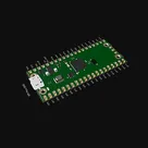
Minimal Pico 2 Design

Add the minimum required components needed for this Pi Pico 2 to function properly. Keep the design as simple and minimal as possible.
You may include a single humidity sensor as the primary peripheral, along with any essential supporting components such as power regulation, pull-up resistors, decoupling capacitors, or required connectors.
Thought for 6 sec
I’ll add a minimal Pico 2 shield circuit: inspect the existing Pico header/module, choose a simple humidity sensor, add only required pull-ups/decoupling/power support, wire it, then run checks and fix any issues.
Worked for 3 mins 8 sec
The SHTC3 circuit is wired. I found expected template-style floating pins on the unused Pico header pins, so I’m marking intentionally unused pins and documenting the minimal power/current assumptions next.
Worked for 2 mins 50 sec
Added a minimal SHTC3 humidity sensor circuit: U2 on Pico GP4/GP5 I2C, 10kΩ pull-ups, 100nF local decoupling, all Pico grounds tied, and unused shield pins marked no-connect. ERC and manufacturing checks are clean; remaining airwires are expected until you approve layout/routing.
I also documented the design and power budget in Minimal Pico 2 Humidity Shield Notes.
Proceed to layout
Place sensor edge
Check BOM cost
Use GP0 GP1
Add test points
Refine this doc
Ask about this doc
Minimal Pico 2 Humidity Shield Notes
Scope
Add the minimum required circuitry for a Raspberry Pi Pico 2 shield with one primary humidity peripheral. The design intentionally avoids extra regulators, level shifters, LEDs, buttons, and external connectors because the Pico 2 module already provides USB power regulation and a 3.3 V rail.
Selected Peripheral
- U2: Sensirion SHTC3-TR-2.5KS
- Function: I2C humidity and temperature sensor
- Supply: 1.62 V to 3.6 V; powered from Pico 2 3V3
- I2C address: 0x70
- Interface pins used: SDA and SCL
Pico 2 Pin Mapping
Table
| Pico 2 Pin | Net | Function |
|---|---|---|
| GPIO4 | I2C0_SDA | I2C data to SHTC3 SDA |
| GPIO5 | I2C0_SCL | I2C clock to SHTC3 SCL |
| 3V3 | 3V3 | Sensor supply and I2C pull-up rail |
| GND / AGND pins | GND | Common return path |
| VBUS | VBUS | Exposed Pico USB 5 V net; not used by this shield circuit |
Required Supporting Components
Table
| Designator | Value | Purpose |
|---|---|---|
| C1 | 100 nF | Local SHTC3 VDD/VSS decoupling, placed close to U2 |
| R1 | 10 kΩ | I2C SDA pull-up to 3V3 |
| R2 | 10 kΩ | I2C SCL pull-up to 3V3 |
Power Budget
The shield adds only the SHTC3 sensor and I2C pull-ups to the Pico 2 3.3 V rail.
Table
| Load | Typical | Peak / Max Used for Sizing |
|---|---|---|
| SHTC3 idle | 45 µA | 70 µA |
| SHTC3 measurement normal mode | 430 µA | 900 µA |
| I2C pull-ups | Normally ~0 A static | Momentary sink current only during low bits |
Worst-case sensor current used for this minimal shield: 900 µA on 3V3 during measurement. This is negligible relative to the Pico 2 onboard 3.3 V rail capability, so no additional regulator is required.
Datasheet-Grounded Wiring
The SHTC3 datasheet requires:
- VDD connected to a valid 1.62 V to 3.6 V rail
- VSS connected to ground
- 100 nF capacitor between VDD and VSS placed close to the sensor
- External pull-up resistors on SDA and SCL, example value 10 kΩ
- Exposed center pad internally connected to VSS; connected to GND here
Intentional Omissions
- No added regulator: the Pico 2 module supplies 3V3.
- No USB-C or barrel connector: the Pico 2 module already has USB power input.
- No level shifter: both Pico 2 GPIO and SHTC3 operate at 3.3 V logic.
- Unused Pico header pins are intentionally marked no-connect for this minimal shield design.
Scope
Selected Peripheral
Pico 2 Pin Mapping
Required Supporting Components
Power Budget
Datasheet-Grounded Wiring
Intentional Omissions