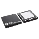
Part Data Review and Validation
Thought for 2 mins 25 sec
I completed the review for TPS274C65ASHRHAR.
Step 1: Part information review
Project metadata vs datasheet
Table
| Item | In part project | Datasheet scan result | Status |
|---|---|---|---|
| MPN | TPS274C65ASHRHAR | TPS274C65ASHRHAR | Match |
| Datasheet URL | Present: PDF | Official TI datasheet | Match |
| Package | Property says TO | RHA, 40-pin VQFN, 6.0 mm x 6.0 mm, 0.5 mm pitch | Mismatch |
| Pin count | 41 schematic terminals including exposed pad | 40 pins + exposed pad | Match |
| Description | "12-V to 36-V 65-mohm four-channel..." | TI describes 72 mOhm quad smart high-side switch | Mismatch |
| Part type | Electromechanical Components | Power switch IC / smart high-side switch | Mismatch |
A datasheet URL was already set on the part, so no web lookup or property update was needed.
Step 3: Datasheet scan summary
Device summary
Table
| Field | Value |
|---|---|
| Function | Quad-channel smart high-side switch with SPI and diagnostics |
| Supply range | 12 V to 36 V nominal operating supply |
| Logic supply | 3.0 V to 5.5 V |
| On-resistance | 72 mOhm typ at 25 C |
| Package | RHA VQFN-40 |
| Body size | 6.0 mm x 6.0 mm |
| Pitch | 0.50 mm |
| Max height | 1.0 mm |
| Variant features | ASH includes reverse current blocking, LED driver, ADC, current sense |
Table
| Feature | Present |
|---|---|
| SPI interface | Yes |
| Adjustable current limit | 290 mA to 2.45 A for ASH |
| Reverse current blocking | Yes |
| LED outputs | 4 |
| Integrated ADC | Yes |
| Current sense | Yes |
| Thermal shutdown | Yes |
| Short-to-ground protection | Yes |
| Wire-break / open-load diagnostics | Yes |
| Short-to-supply detection | Yes |
Table
| Parameter | Rating |
|---|---|
| VS continuous | -0.3 V to 40 V |
| VS transient under 1 ms during ON state | -0.3 V to 60 V |
| VOUT to GND | -30 V to VS + 0.3 V |
| VDS | -0.7 V to 39 V |
| VDD | -0.3 V to 7.0 V |
| Digital input pins | -0.3 V to 7.0 V |
| LED output pins | -0.3 V to 7.0 V |
| REG_EN | -0.3 V to 7.0 V |
| RCBx | VOUT - 0.7 V to VOUT + 6 V |
| ISNS | -0.3 V to 7.0 V |
| FLT | -0.3 V to 7.0 V |
| Reverse ground current | -50 mA |
| Junction temperature | 150 C max |
| Storage temperature | -65 C to 150 C |
Table
| Parameter | Range |
|---|---|
| VS nominal supply | 12 V to 36 V |
| VDD | 3.0 V to 5.5 V |
| Digital input pins | -0.3 V to 5.5 V |
| FLT pin | -0.3 V to 5.5 V |
| LEDOUT pins | -0.3 V to 5.5 V |
| REG_EN | -0.3 V to 5.0 V |
| Operating ambient from orderable info | -40 C to 125 C |
Table
| Parameter | Value |
|---|---|
| On-resistance RON | 72 mOhm typ at 25 C, 110 mOhm typ at 125 C |
| Parallel 2-channel RON | 33 mOhm typ at 25 C, 55 mOhm typ at 125 C |
| Internal VDD regulator output | 3.1 V min, 3.3 V typ, 3.6 V max |
| Internal VDD regulator current limit | 25 mA min, 50 mA max |
| Continuous load current per channel | 1.6 A typ with all channels on at 85 C |
| Continuous load current per channel | 2.5 A typ with two channels on at 85 C |
| VDD quiescent current | 1.0 mA typ to 1.3 mA typ depending condition |
| VS quiescent current | 1.4 mA typ to 2.8 mA typ depending condition |
| Current sense ratio IOUT / ISNS | 1160 typ |
| ADC reference | 2.72 V min, 2.8 V typ, 2.85 V max |
| ADC conversion update time | 128 us typ |
| Thermal shutdown warning | 110 C min, 130 C typ, 150 C max |
| Thermal shutdown | 160 C min, 185 C typ, 210 C max |
Table
| Pin(s) | Signal(s) | Datasheet role |
|---|---|---|
| 1 | ~READY | Ready/status output |
| 2 | ~FLT | Open-drain fault output |
| 3 | DO_EN | Global output enable input |
| 4 | VDD | Logic supply input |
| 5, 21 | GND_1, GND_2 | Ground |
| 6 | ISNS | Analog current-sense output |
| 7 | SDO | SPI data output |
| 8 | SDI | SPI data input |
| 9 | SCLK | SPI clock input |
| 10 | ~CS | SPI chip select input |
| 11 | RCB3 | Reverse current blocking gate for channel 3 |
| 12, 13 | OUT3_1, OUT3_2 | Channel 3 output |
| 14-17 | VS_1, VS_2, VS_3, VS_4 | Main switch supply input |
| 18, 19 | OUT4_1, OUT4_2 | Channel 4 output |
| 20 | RCB4 | Reverse current blocking gate for channel 4 |
| 22-25 | LEDOUT1, LEDOUT2, LEDOUT3, LEDOUT4 | LED matrix driver outputs |
| 26, 27 | DNC_1, DNC_2 | Do not connect |
| 28 | DSPI | Daisy-chain SPI mode input |
| 29 | REG_EN | Internal regulator enable |
| 30 | ADDCFG | SPI address configuration |
| 31 | RCB2 | Reverse current blocking gate for channel 2 |
| 32, 33 | OUT2_1, OUT2_2 | Channel 2 output |
| 34-37 | VS_5, VS_6, VS_7, VS_8 | Main switch supply input |
| 38, 39 | OUT1_1, OUT1_2 | Channel 1 output |
| 40 | RCB1 | Reverse current blocking gate for channel 1 |
| EP | EP | Exposed pad, connect to IC ground |
Table
| Parameter | Datasheet value |
|---|---|
| Package code | RHA0040M |
| Package type | VQFN-40 |
| Body size A x B | 5.9 mm to 6.1 mm square |
| Exposed pad D2 x E2 | 4.15 mm +/- 0.1 mm |
| Lead pitch e | 0.50 mm |
| Terminal width b | 0.20 mm to 0.30 mm |
| Terminal length L | 0.30 mm to 0.50 mm |
| Height A | 0.8 mm to 1.0 mm |
| TI example land pattern terminal size | 40x 0.25 mm x 0.6 mm |
| TI example exposed pad land | 4.15 mm square |
Table
| Check | Result | Risk |
|---|---|---|
| Pin count | 41 terminals in project = 40 pins + exposed pad | OK |
| Pin numbering | Matches datasheet numbering including EP as 41 | OK |
| Pin names | AS/ASH pin names align with datasheet | OK |
| DNC pins | DNC_1 and DNC_2 present | OK |
| Footprint package family | Footprint filename indicates QFN50P600X600X100-41N-D, consistent with 0.5 mm pitch, 6x6 mm, 1.0 mm height, 41 terminals incl. EP | OK |
| Exposed pad present | EP and pad 41 exist | OK |
| Metadata package property | Project says TO instead of RHA / VQFN-40 | Ordering/library risk |
| Metadata part type | Project says Electromechanical Components | Library/search/BOM risk |
| Description value | Project says 65-mohm, datasheet says 72 mOhm typ | Specification risk |
| Symbol pin electrical types | All terminals are marked Unspecified in the symbol | ERC/usability risk |
| Footprint peripheral pad length | Footprint uses 0.25 mm x 0.85 mm pads, TI example land pattern shows 0.25 mm x 0.6 mm | Manufacturing risk |
| Exposed pad size | Footprint EP is 4.25 mm square, TI example land is 4.15 mm | Minor assembly review item |
Table
| Priority | Issue | Why it matters |
|---|---|---|
| High | Peripheral pads appear 0.85 mm long instead of TI's 0.6 mm recommendation | On a 0.5 mm pitch VQFN, longer pads can increase solder bridging and skew assembly yield |
| High | Package property is TO | Can cause wrong package identification and wrong ordering assumptions |
| Medium | Description says 65-mohm instead of 72 mOhm typ | Can mislead selection and review |
| Medium | Part type is incorrect | Can affect organization, filtering, and part reuse |
| Medium | All symbol pins are Unspecified rather than input/output/power/ground | Can weaken ERC quality and make the part harder to use safely |
| Low | Exposed pad land is 4.25 mm vs TI example 4.15 mm | Usually not fatal, but worth reviewing with stencil/paste strategy |
- The pin map is good and matches the ASH datasheet.
- The footprint family is broadly correct for a 6 mm x 6 mm, 0.5 mm pitch VQFN-40 with EP.
- The biggest concern is the outer pad length mismatch versus TI's recommended land pattern.
- The project metadata also has clear package/type/spec mismatches that should be corrected before reuse or release.
If you want, I can next give you a precise fix list for the part project fields and footprint dimensions.
Fix list next
Check pin types
Review DRC risks
Name
Pin #
Type
Part Type
Terminal Order
~READY
1
Unspecified
Terminal
~FLT
2
Unspecified
Terminal
DO_EN
3
Unspecified
Terminal
VDD
4
Unspecified
Terminal
GND_1
5
Unspecified
Terminal
ISNS
6
Unspecified
Terminal
SDO
7
Unspecified
Terminal
SDI
8
Unspecified
Terminal
SCLK
9
Unspecified
Terminal
~CS
10
Unspecified
Terminal
RCB3
11
Unspecified
Terminal
OUT3_1
12
Unspecified
Terminal
OUT3_2
13
Unspecified
Terminal
VS_1
14
Unspecified
Terminal
VS_2
15
Unspecified
Terminal
VS_3
16
Unspecified
Terminal
VS_4
17
Unspecified
Terminal
OUT4_1
18
Unspecified
Terminal
TPS274C65ASHRHAR