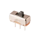
Part Datasheet Analysis and Validation
Thought for 4 mins 10 sec
Here’s the complete execution of your 4-step request.
- Part information review (current project)
- Part: SLW-883935-2A-D
- Description: “8.8 x 3.9 x 3.5 mm, 2 mm Raised Slide Actuator, Right-Angle, Through Hole, Slide Switch”
- Manufacturer: Same Sky
- MPN: SLW-883935-2A-D
- Mount: Through Hole; Orientation: Right-angle
- Designator Prefix: S
- Pin count (from symbol): 3
- Schematic pins in symbol:
- Datasheet URL property present: https://www.sameskydevices.com/product/resource/SLW-883935-2A-D.pdf
- Datasheet check/update
- A datasheet URL is already set on this part. No change required.
- Datasheet scan and metadata extraction Datasheet: https://www.sameskydevices.com/product/resource/SLW-883935-2A-D.pdf
Electrical and ratings
- Rated voltage: 30 Vdc
- Rated current: 500 mA
- Withstanding voltage: 250 Vac (for 1 minute)
- Contact resistance: 100 mΩ max (measured at 1 kHz at 100 mA or less)
- Insulation resistance: 100 MΩ (at 100 Vdc for 1 minute)
- Switch function: SPDT (non-shorting)
Operating and environmental
- Operating temperature: -20 to 70 °C
- Storage temperature: -40 to 90 °C
- Life (no load): 10,000 cycles (at 15–18 cycles per minute)
- Vibration: 10–55–10 Hz, 1.5 mm amplitude, 2 hours on each X/Y/Z
Mechanical characteristics
- Operating force: 100 gf min / 200 gf typ / 300 gf max
- Actuator travel: 1.7 mm min / 2.0 mm typ / 2.3 mm max
- Features: through hole, raised slide actuator
Materials and compliance
- Terminal: brass, silver plating
- Contact: PBS, silver plating
- RoHS: yes
- Flammability rating: see material table (not detailed in extracted text)
Soldering recommendations
- Hand soldering: 350 °C max, 3 s max
- Wave soldering: 260 °C max, 5 s max
Package dimensions and recommended PCB layout (Top View)
- Package dims: Mechanical drawing provided (units mm, ±0.20 mm unless noted)
- Recommended PCB layout (numeric):
- Hole diameter: 0.8 mm
- Center-to-center spacing (adjacent holes): 2.5 mm
- Center-to-center spacing (outer holes): 5.0 mm
- Notes: Datasheet includes “SCHEMATIC SPDT (NON-SHORTING)” and “Recommended PCB Layout (Top View)”. No explicit terminal numbering text was found in the extracted content.
- Cross-check: schematic symbol and footprint vs datasheet
Symbol
- Present pins: NC (Pin 1), COM (Pin 2), NO (Pin 3) — matches an SPDT function and names expected from the datasheet’s “SPDT (Non-shorting)”.
- Issue: Pin Type for all three pins is “Unspecified”. For a mechanical switch, these should be Passive to avoid ERC pin-type conflicts.
Footprint
- Pads present in layout: COM, NO, NC (3 pads), matching the 3-pin SPDT function.
- Expected from datasheet:
- Through-hole pads with recommended drill of 0.8 mm
- Hole spacing: 2.5 mm between adjacent holes, 5.0 mm total between outer holes
- What I can confirm from the project:
- Pad names (COM/NO/NC) exist in the footprint.
- The layout tool did not expose pad coordinates/diameters in the current view, so I cannot numerically verify drill size and center spacing against the datasheet from tool output alone.
- Actionable flags:
- Verify pad drill = 0.8 mm and pad center spacing = 2.5/5.0 mm to match the datasheet’s recommended PCB layout.
- Confirm footprint orientation matches right-angle configuration so the actuator direction aligns with board edge and mechanical keepouts.
Additional recommendations to avoid ordering/manufacturing errors
- Document electrical ratings in the part properties for clarity (Rated Voltage: 30 Vdc, Rated Current: 500 mA).
- Consider adding life-cycle and soldering notes (hand: 350 °C/3 s; wave: 260 °C/5 s) to the part’s documentation, if you keep process constraints at the part level.
- If pad geometry differs from 0.8 mm drill and 2.5/5.0 mm spacing, update the footprint to the datasheet’s recommended PCB layout to ensure fit.
Summary of flags
- Schematic pin types: set NC, COM, NO to Passive.
- Footprint pad geometry: confirm drills and spacing match 0.8 mm drill, 2.5/5.0 mm spacing; current tool output did not include numeric geometry to auto-verify.
- Orientation: visually confirm right-angle actuator alignment relative to board edge per mechanical drawing.
If you want, I can attempt to set the pin types to Passive and add the key ratings as part properties.
Check pad drill/spacing
Set pins to Passive
Add ratings to properties
Verify footprint orientation