Part Review and Datasheet Validation
Thought for 3 mins 27 sec
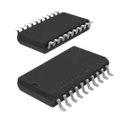
Part review summary for MAX7219CWG+T
Datasheet metadata extracted
Absolute maximum ratings
Recommended operating conditions
Key electrical characteristics
Pin functions confirmed from datasheet
Package dimensions from datasheet
Symbol and footprint cross-check
What matches
Issues that should be fixed
Potential pin-mapping concern
Bottom line
Step 2 did not require action because this part project already has a datasheet URL set:
http://componentsearchengine.com/Datasheets/1/MAX7219CWG+T.pdf
Table
| Field | Value |
|---|---|
| MPN | MAX7219CWG+T |
| Manufacturer | Analog Devices |
| Description | Serially interfaced, 8-digit LED display driver |
| Package in project | 24-pin Wide SO / SOIC |
| Footprint asset | SOIC127P1032X265-24N.kicad_mod |
| 3D model asset | MAX7219CWG+T.stp |
| Schematic pin count | 24 |
| Footprint pad count | 24 |
Table
| Category | Extracted data |
|---|---|
| Device type | Serial input/output common-cathode LED display driver for up to 8 digits, bar graphs, or 64 LEDs |
| Interface | 10 MHz serial interface |
| Internal functions | BCD code-B decoder, multiplex scan circuitry, segment and digit drivers, 8x8 static RAM |
| LED current programming | One external resistor on ISET sets peak segment current |
| Brightness control | Digital and analog brightness control |
| Startup behavior | Display blanked on power-up; enters shutdown on initial power-up |
| Shutdown current | 150 µA low-power shutdown, with data retained |
| Display control registers | Decode mode, intensity, scan limit, shutdown, display test |
| Display range | Scan-limit register supports 1 to 8 digits |
| Special note | MAX7221 variant adds slew-rate-limited drivers and SPI/QSPI/MICROWIRE compatibility; this is not a MAX7219-only feature |
Table
| Parameter | Rating |
|---|---|
| V+ to GND | -0.3 V to 6 V |
| DIN, CLK, LOAD, CS to GND | -0.3 V to 6 V |
| All other pins | -0.3 V to (V+ + 0.3 V) |
| DIG0-DIG7 sink current | 500 mA |
| SEG A-G, DP source current | 100 mA |
| Continuous power dissipation, Wide SO at TA = +85°C | 941 mW |
| Wide SO derating above +70°C | 11.8 mW/°C |
| Storage temperature | -65°C to +160°C |
| Lead temperature, soldering 10 s | +300°C |
Table
| Parameter | Value |
|---|---|
| Operating supply voltage V+ | 4.0 V min, 5.5 V max |
| Operating temperature, MAX7219C_G | 0°C to +70°C |
| Operating temperature, MAX7219E_G | -40°C to +85°C |
| Segment drive source current ISEG | -30 mA min, -40 mA typ, -45 mA max |
| Maximum recommended segment current | 40 mA |
Table
| Parameter | Value |
|---|---|
| Logic high input voltage VIH | 3.5 V min |
| Logic low input voltage VIL | 0.8 V max |
| Input current IIH / IIL | -1 µA to 1 µA |
| Output low voltage VOL | 0.4 V |
| Output high voltage VOH | V+ - 1 V |
| Hysteresis on DIN/CLK/LOAD/CS | 1 V |
| Clock period tCP | 100 ns min |
| CLK high pulse width tCH | 50 ns min |
| CLK low pulse width tCL | 50 ns min |
| DIN setup time tDS | 25 ns min |
| DIN hold time tDH | 0 ns min |
| LOAD/CS pulse high tCSW | 50 ns min |
| Data propagation delay tDO | 25 ns |
| Data-to-segment delay tDSPD | 2.25 ms |
| Digit drive sink current IDIGIT | 320 mA |
| Display scan rate | 500 Hz min, 800 Hz typ, 1300 Hz max |
| Segment current matching | 3.0% |
Table
| Pin / Function | Datasheet summary |
|---|---|
| DIN | Serial-data input, sampled on CLK rising edge |
| DOUT | Serial-data output, valid 16.5 clock cycles later, used for daisy chaining |
| CLK | Serial clock input, 10 MHz max |
| LOAD / CS | Latches the last 16 bits on rising edge |
| DIG0-DIG7 | Digit drive outputs, sink current from common-cathode display |
| SEG A-G, DP | Segment outputs, source current to LED segments |
| ISET | Connect through resistor to VDD/V+ to set peak segment current |
| V+ | Positive supply, connect to +5 V |
| GND pins | Both grounds must be connected |
Table
| Parameter | 24 Wide SO |
|---|---|
| Body length D | 15.20 mm to 15.60 mm |
| Body width E | 7.40 mm to 7.60 mm |
| Lead span H | 10.00 mm to 10.65 mm |
| Overall height A | 2.35 mm to 2.65 mm |
| Standoff A1 | 0.10 mm to 0.32 mm |
| Lead width B | 0.23 mm to 0.35 mm |
| Lead thickness C | 0.30 mm to 0.49 mm |
| Lead pitch e | 1.27 mm |
| Lead length L | 0.40 mm to 1.27 mm |
| Lead angle | 0° to 8° |
Table
| Check | Result |
|---|---|
| Pin count | Pass - symbol exposes 24 terminals and footprint has 24 pads |
| Package family | Pass - project uses a 24 Wide SO / SOIC footprint, matching datasheet ordering info for MAX7219CWG |
| Pitch | Pass - footprint is 1.27 mm pitch, matching datasheet |
| Body size | Pass - footprint body is about 15.4 mm x 7.5 mm, matching datasheet ranges for D and E |
| 3D model presence | Pass - 3D model asset is attached |
Table
| Issue | Risk | Evidence |
|---|---|---|
| All symbol pins are typed as Unspecified | ERC quality and downstream part quality are degraded | Every terminal in the schematic is currently Pin Type: Unspecified |
| Symbol uses generic terminal parts instead of a unified IC symbol | Higher chance of incorrect reuse and weaker readability | The schematic consists of 24 separate terminal objects such as DIN, CLK, DOUT, V |
| Ground pins are split into two separately named terminals, GND_1 and GND_2 | Can cause incorrect symbol semantics and easier wiring mistakes in reuse | Datasheet explicitly states both GND pins must be connected |
| No visible net validation yet | Real connectivity errors would not be caught from this part project alone | Project schematic currently reports no nets defined yet |
I do not see a clear manufacturing-footprint mismatch from the current data. The footprint geometry looks consistent with the datasheet package.
However, there is one thing to verify carefully before releasing this as a reusable part:
- The datasheet text extraction for the pin table is slightly inconsistent in OCR formatting, while the current symbol pin numbering appears internally consistent with the expected MAX7219 arrangement.
- Because of that, I would treat the pin-number-to-pin-name mapping as mostly consistent but worth one final manual verification against the datasheet top-view before publishing broadly.
Table
| Category | Status |
|---|---|
| Wrong package ordered | Low risk - package and footprint family match |
| Footprint dimensional mismatch | Low risk - dimensions and pitch align well |
| Solderability risk from pad geometry | Low risk from current evidence |
| Board failure from package mismatch | Low risk from current evidence |
| Board failure from symbol pin-type / symbol-quality issues | Moderate risk for reuse and wiring mistakes |
| Need final pin-map sanity check | Yes |
- The package selection and footprint look correct for MAX7219CWG+T.
- The main weaknesses are in the symbol quality, not the footprint:
- pin electrical types are missing
- the symbol is built from separate terminals rather than a clean IC symbol
- the two grounds should be clearly represented as required by the datasheet
- I do not see a strong sign of a manufacturing-breaking footprint error, but I do recommend a final pin-map verification before using this part in hardware.
Check pin mapping
Review ERC issues
Create proper symbol
Name
Pin #
Type
Part Type
Terminal Order
DIN
1
Unspecified
Terminal
DIG0
2
Unspecified
Terminal
DIG4
3
Unspecified
Terminal
GND_1
4
Unspecified
Terminal
DIG6
5
Unspecified
Terminal
DIG2
6
Unspecified
Terminal
DIG3
7
Unspecified
Terminal
DIG7
8
Unspecified
Terminal
GND_2
9
Unspecified
Terminal
DIG5
10
Unspecified
Terminal
DIG1
11
Unspecified
Terminal
LOAD
12
Unspecified
Terminal
CLK
13
Unspecified
Terminal
SEG_A
14
Unspecified
Terminal
SEG_F
15
Unspecified
Terminal
SEG_B
16
Unspecified
Terminal
SEG_G
17
Unspecified
Terminal
ISET
18
Unspecified
Terminal
MAX7219CWG+T